Skip to content
Jason Kridner edited this page May 6, 2020 · 4 revisions

imageimageREF: BBONEBLK_SRM BeagleBone Black System Rev C.1

___________________ *Reference Manual * ___________________ image:media2/media/image3.jpeg[image,width=568,height=346] *BeagleBone Black* _________________________ *System Reference Manual* _________________________ [[revision-c.1-may-22-2014]] Revision C.1 May 22, 2014 +++++++++++++++++++++++++ ____________________________________________________________________________________________________________________________________________________________________ *Author: Gerald Coley gerald@beagleboard.org* *Contributing Editor: Robert P J Day* image:media2/media/image1.png[image,width=194,height=34]image:media2/media/image2.jpeg[image,width=172,height=27]*REF: BBONEBLK_SRM BeagleBone Black System Rev C.1* *Reference Manual * ____________________________________________________________________________________________________________________________________________________________________ *THIS DOCUMENT* ___________________________________________________________________________________________________________________________________________________________________________________________________________________________________________________________________________________________________________________________________________________________________________________________________ __This work is licensed under the Creative Commons Attribution-Share Alike 3.0 Unported License. To view a copy of this license, visit http://creativecommons.org/licenses/by-sa/3.0/[http://creativecommons.org/licenses/by-] http://creativecommons.org/licenses/by-sa/3.0/[sa/3.0/] or send a letter to Creative Commons, 171 Second Street, Suite 300, San Francisco, California, 94105, USA.__ __All derivative works are to be attributed to Gerald Coley of BeagleBoard.org.__ __For more information, see http://creativecommons.org/license/results-one?license_code=by-sa[http://creativecommons.org/license/results-] http://creativecommons.org/license/results-one?license_code=by-sa[one?license_code=by-sa]__ ___________________________________________________________________________________________________________________________________________________________________________________________________________________________________________________________________________________________________________________________________________________________________________________________________ [[send-all-comments-and-errors-concerning-this-document-to-the-author-at-geraldbeagleboard.org]] Send all comments and errors concerning this document to the author at gerald@beagleboard.org +++++++++++++++++++++++++++++++++++++++++++++++++++++++++++++++++++++++++++++++++++++++++++++ *For other questions you may contact Gerald at:* _________________________________________________ *Gerald Coley Texas Instruments* *12500 TI Blvd. Dallas, Tx 75243 g-coley1@ti.com* _________________________________________________ *All information in this document is subject to change without notice.* *For an up to date version of this document refer to:* *http://circuitco.com/support/index.php?title=BeagleBoneBlack&LATEST_PRODUCTION_FILES_.28A5A.29[http://circuitco.com/support/index.php?title=BeagleBoneBlack#LATEST_PRODUC] http://circuitco.com/support/index.php?title=BeagleBoneBlack&LATEST_PRODUCTION_FILES_.28A5A.29[TION_FILES_.28A5A.29]* _____________________________________________________________________________________________________________________________________________________________________________________________________________________________________________________________________________________________________________________________________________________________________________________________________________________________________________________________________________________________________________________________________________________________________________________________________ image:media2/media/image1.png[image,width=194,height=34]image:media2/media/image2.jpeg[image,width=172,height=27]*REF: BBONEBLK_SRM BeagleBone Black System Rev C.1* *Reference Manual * *BEAGLEBONE DESIGN* These design materials referred to in this document are **NOT SUPPORTED** and *DO NOT* constitute a reference design. Only “community” support is allowed via resources at http://beagleboard.org/discuss[_BeagleBoard.org/discuss._] THERE IS NO WARRANTY FOR THE DESIGN MATERIALS, TO THE EXTENT PERMITTED BY APPLICABLE LAW. EXCEPT WHEN OTHERWISE STATED IN WRITING THE COPYRIGHT HOLDERS AND/OR OTHER PARTIES PROVIDE THE DESIGN MATERIALS “AS IS” WITHOUT WARRANTY OF ANY KIND, EITHER EXPRESSED OR IMPLIED, INCLUDING, BUT NOT LIMITED TO, THE IMPLIED WARRANTIES OF MERCHANTABILITY AND FITNESS FOR A PARTICULAR PURPOSE. THE ENTIRE RISK AS TO THE QUALITY AND PERFORMANCE OF THE DESIGN MATERIALS IS WITH YOU. SHOULD THE DESIGN MATERIALS PROVE DEFECTIVE, YOU ASSUME THE COST OF ALL NECESSARY SERVICING, REPAIR OR CORRECTION. This board was designed as an evaluation and development tool. It was not designed with any other application in mind. As such, the design materials that are provided which include schematic, BOM, and PCB files, may or may not be suitable for any other purposes. If used, the design material becomes your responsibility as to whether or not it meets your specific needs or your specific applications and may require changes to meet your requirements. _____________________________________________________________________________________________________________________________________________________________________________________________________________________________________________________________________________________________________________________________________________________________________________________________________________________________________________________________________________________________________________________________________________________________________________________________________ [[ref-bboneblk_srm-beaglebone-black-system-rev-c.1-1]] image:media2/media/image1.png[image,width=194,height=34]image:media2/media/image2.jpeg[image,width=172,height=27]REF: BBONEBLK_SRM BeagleBone Black System Rev C.1

*Reference Manual *

BEAGLEBONE BLACK ADDITIONAL TERMS

BeagleBoard.org, Circuitco, LLC, and BeagleBoard.org (Supplier) provide the enclosed BeagleBone under the following conditions:

The user assumes all responsibility and liability for proper and safe handling of the goods. Further, the user indemnifies Supplier from all claims arising from the handling or use of the goods.

Should the BeagleBone not meet the specifications indicated in the System Reference Manual, the BeagleBone may be returned within 90 days from the date of delivery to the distributor of purchase for a full refund. THE FOREGOING LIMITED WARRANTY IS THE EXCLUSIVE WARRANTY MADE BY SELLER TO BUYER AND IS IN LIEU OF ALL OTHER WARRANTIES, EXPRESSED, IMPLIED, OR STATUTORY, INCLUDING ANY WARRANTY OF MERCHANTABILITY OR FITNESS FOR ANY PARTICULAR PURPOSE. EXCEPT TO THE EXTENT OF THE INDEMNITY SET FORTH ABOVE, NEITHER PARTY SHALL BE LIABLE TO THE OTHER FOR ANY INDIRECT, SPECIAL, INCIDENTAL, OR CONSEQUENTIAL DAMAGES.

Please read the System Reference Manual and, specifically, the Warnings and Restrictions notice in the Systems Reference Manual prior to handling the product. This notice contains important safety information about temperatures and voltages.

No license is granted under any patent right or other intellectual property right of Supplier covering or relating to any machine, process, or combination in which such Supplier products or services might be or are used. The Supplier currently deals with a variety of customers for products, and therefore our arrangement with the user is not exclusive. The Supplier assume no liability for applications assistance, customer product design, software performance, or infringement of patents or services described herein.

UNITED STATES FCC AND CANADA IC REGULATORY COMPLIANCE INFORMATION

The BeagleBone is annotated to comply with Part 15 of the FCC Rules. Operation is subject to the following two conditions: (1) This device may not cause harmful interference, and (2) this device must accept any interference received, including interference that may cause undesired operation. Changes or modifications not expressly approved by the party responsible for compliance could void the user’s authority to operate the equipment.

This Class A or B digital apparatus complies with Canadian ICES-003. Changes or modifications not expressly approved by the party responsible for compliance could void the user’s authority to operate the equipment. Cet appareil numérique de la classe A ou B est conforme à la norme NMB-003 du Canada. Les changements ou les modifications pas expressément approuvés par la partie responsible de la conformité ont pu vider l’autorité de l’utilisateur pour actionner l’équipement.

imageimageREF: BBONEBLK_SRM BeagleBone Black System Rev C.1

__________________________________________________________________________________________________________________________________________________________________________________________________________________________________________________________________________________________________________________________________________________________________________________________________________________________________________________________________________________________________________ *Reference Manual * *BEAGLEBONE WARNINGS, RESTRICTIONS AND DISCLAIMERS* _*For Feasibility Evaluation Only, in Laboratory/Development Environments*. The_ _BeagleBone Black is not a complete product. It is intended solely for use for preliminary_ _feasibility evaluation in laboratory/development environments by technically qualified_ _electronics experts who are familiar with the dangers and application risks associated with_ _handling electrical mechanical components, systems and subsystems. It should not be_ _used as all or part of a finished end product._ **Your Sole Responsibility and Ris**k you acknowledge, represent, and agree that: __________________________________________________________________________________________________________________________________________________________________________________________________________________________________________________________________________________________________________________________________________________________________________________________________________________________________________________________________________________________________________ 1. You have unique knowledge concerning Federal, State and local regulatory requirements (including but not limited to Food and Drug Administration regulations, if applicable) which relate to your products and which relate to your use (and/or that of your employees, affiliates, contractors or designees) of the BeagleBone for evaluation, testing and other purposes. 2. You have full and exclusive responsibility to assure the safety and compliance of your products with all such laws and other applicable regulatory requirements, and also to assure the safety of any activities to be conducted by you and/or your employees, affiliates, contractors or designees, using the BeagleBone. Further, you are responsible to assure that any interfaces (electronic and/or mechanical) between the BeagleBone and any human body are designed with suitable isolation and means to safely limit accessible leakage currents to minimize the risk of electrical shock hazard. 3. Since the BeagleBone is not a completed product, it may not meet all applicable regulatory and safety compliance standards which may normally be associated with similar items. You assume full responsibility to determine and/or assure compliance with any such standards and related certifications as may be applicable. You will employ reasonable safeguards to ensure that your use of the BeagleBone will not result in any property damage, injury or death, even if the BeagleBone should fail to perform as described or expected. _____________________________________________________________________________________________________________________________________________________________________________________________________________________________________________________________________________________________________________________________________________________________________________________________________________________________________________________________________________________________________________________________________________________________________________________________________________________________________________________________________________________________________________________________________________________________________________________________________________________________________________________________________________________________________________________________________________________________________________________________________________________________________________________________________________________________________________________________________________________________________________________________________________________________________________________________________________________________________________________________________________________________________________________________________________________________________________________________________________________________________________________________________________________________________________________________________________________________________________________________________________________________________________________________________________________________________________________________________ _*Certain Instructions*. It is important to operate the BeagleBone Black within Supplier’s_ _recommended specifications and environmental considerations per the user guidelines._ _Exceeding the specified BeagleBone ratings (including but not limited to input and output_ _voltage, current, power, and environmental ranges) may cause property damage, personal_ injury or death. If there are questions concerning these ratings please contact the Supplier _representative prior to connecting interface electronics including input power and intended_ loads. Any loads applied outside of the specified output range may result in unintended _and/or inaccurate operation and/or possible permanent damage to the BeagleBone and/or_ interface electronics. Please consult the System Reference Manual prior to connecting any load to the BeagleBone output. If there is uncertainty as to the load specification, please _contact the Supplier representative. During normal operation, some circuit components_ _may have case temperatures greater than 60 C as long as the input and output are_ _maintained at a normal ambient operating temperature. These components include but are_ _not limited to linear regulators, switching transistors, pass transistors, and current sense_ _resistors which can be identified using the BeagleBone schematic located at the link in the_ _BeagleBone System Reference Manual. When placing measurement probes near these_ _devices during normal operation, please be aware that these devices may be very warm to_ _the touch. As with all electronic evaluation tools, only qualified personnel knowledgeable in_ _electronic measurement and diagnostics normally found in development environments_ _should use the BeagleBone._ _*Agreement to Defend, Indemnify and Hold Harmless*. You agree to defend, indemnify_ _and hold the Suppliers, its licensors and their representatives harmless from and against_ _any and all claims, damages, losses, expenses, costs and liabilities (collectively,_ _"Claims") arising out of or in connection with any use of the BeagleBone that is not in_ _____________________________________________________________________________________________________________________________________________________________________________________________________________________________________________________________________________________________________________________________________________________________________________________________________________________________________________________________________________________________________________________________________________________________________________________________________________________________________________________________________________________________________________________________________________________________________________________________________________________________________________________________________________________________________________________________________________________________________________________________________________________________________________________________________________________________________________________________________________________________________________________________________________________________________________________________________________________________________________________________________________________________________________________________________________________________________________________________________________________________________________________________________________________________________________________________________________________________________________________________________________________________________________________________________________________________________________________________________ [[ref-bboneblk_srm-beaglebone-black-system-rev-c.1-3]] image:media2/media/image1.png[image,width=194,height=34]image:media2/media/image2.jpeg[image,width=172,height=27]REF: BBONEBLK_SRM BeagleBone Black System Rev C.1

*Reference Manual *

accordance with the terms of the agreement. This obligation shall apply whether Claims arise under law of tort or contract or any other legal theory, and even if the BeagleBone fails to perform as described or expected.

*Safety-Critical or Life-Critical Applications*. If you intend to evaluate the components for possible use in safety critical applications (such as life support) where a failure of the Supplier’s product would reasonably be expected to cause severe personal injury or death, such as devices which are classified as FDA Class III or similar classification, then you must specifically notify Suppliers of such intent and enter into a separate Assurance and Indemnity Agreement.

Mailing Address:

BeagleBoard.org

1380 Presidential Dr. #100

Richardson, TX 75081

U.S.A.

WARRANTY: The BeagleBone Black Assembly as purchased is warranted against defects in materials and workmanship for a period of 90 days from purchase. This warranty does not cover any problems occurring as a result of improper use, modifications, exposure to water, excessive voltages, abuse, or accidents. All boards will be returned via standard mail if an issue is found. If no issue is found or express return is needed, the customer will pay all shipping costs.

Before returning the board, please visit BeagleBoard.org/support

For up to date SW images and technical information refer to http://circuitco.com/support/index.php?title=BeagleBoneBlack

All support for this board is provided via community support at www.beagleboard.org/discuss

To return a defective board for repair, please request an RMA at http://beagleboard.org/support/rma

Please DO NOT return the board without approval from the RMA team first.

All boards received without RMA approval will not be worked on.

imageimageREF: BBONEBLK_SRM BeagleBone Black System Rev C.1

*Reference Manual * Table of Contents [[figures]] Figures ------- _________________________________________________________________________________ link:#_bookmark16[Figure 1. In The Box 17] link:#_bookmark19[Figure 2. Tethered Configuration 18] link:#_bookmark21[Figure 3. USB Connection to the Board 19] link:#_bookmark22[Figure 4. Board Power LED 19] link:#_bookmark23[Figure 5. Board Boot Status 20] link:#_bookmark26[Figure 6. Desktop Configuration 21] link:#_bookmark29[Figure 7. Connect microHDMI Cable to the Monitor 22] link:#_bookmark30[Figure 8. DVI-D to HDMI Adapter 22] link:#_bookmark31[Figure 9. Wireless Keyboard and Mouse Combo 23] link:#_bookmark32[Figure 10. Connect Keyboard and Mouse Receiver to the Board 23] link:#_bookmark33[Figure 11. Keyboard and Mouse Hubs 23] link:#_bookmark34[Figure 12. Ethernet Cable Connection 24] link:#_bookmark36[Figure 13. External DC Power 24] link:#_bookmark37[Figure 14. Connect microHDMI Cable to the Board 25] link:#_bookmark38[Figure 15. Board Boot Status 25] link:#_bookmark39[Figure 16. Desktop Screen 26] link:#_bookmark46[Figure 17. Connectors, LEDs and Switches 31] link:#_bookmark48[Figure 18. Key Components 32] link:#_bookmark51[Figure 19. BeagleBone Black Key Components 33] link:#_bookmark71[Figure 20. BeagleBone Black Block Diagram 40] link:#_bookmark73[Figure 21. High Level Power Block Diagram 41] link:#_bookmark75[Figure 22. TPS65217C Block Diagram 43] link:#_bookmark77[Figure 23. TPS65217 DC Connection 44] link:#_bookmark79[Figure 24. USB Power Connections 45] link:#_bookmark88[Figure 25. Power Rails 49] link:#_bookmark89[Figure 26. Power Rail Power Up Sequencing 51] link:#_bookmark90[Figure 27. TPS65217C Power Sequencing Timing 52] link:#_bookmark93[Figure 28. Power Processor Interfaces 52] link:#_bookmark98[Figure 29. Sitara AM3358BZCZ Block Diagram 55] link:#_bookmark103[Figure 30. Processor Crystals 57] link:#_bookmark105[Figure 31. Board Reset Circuitry 58] link:#_bookmark108[Figure 32. DDR3L Memory Design 60] link:#_bookmark111[Figure 33. DDR3L VREF Design 61] link:#_bookmark115[Figure 34. eMMC Memory Design 63] link:#_bookmark119[Figure 35. EEPROM Design Rev A5 65] link:#_bookmark122[Figure 36. microSD Design 65] _________________________________________________________________________________ [[ref-bboneblk_srm-beaglebone-black-system-rev-c.1-5]] image:media2/media/image1.png[image,width=194,height=34]image:media2/media/image2.jpeg[image,width=172,height=27]REF: BBONEBLK_SRM BeagleBone Black System Rev C.1

Reference Manual

imageimageREF: BBONEBLK_SRM BeagleBone Black System Rev C.1

*Reference Manual * [[tables]] Tables ------ ________________________________________________________________________ link:#_bookmark5[Table 1. Change History 14] link:#_bookmark43[Table 2. BeagleBone Black Features 30] link:#_bookmark83[Table 3. BeagleBone Black Battery Pins 46] link:#_bookmark85[Table 4. BeagleBone Black Power Consumption(mA@5V) 47] link:#_bookmark100[Table 5. Processor Features 56] link:#_bookmark116[Table 6. eMMC Boot Pins 63] link:#_bookmark118[Table 7. EEPROM Contents 64] link:#_bookmark125[Table 8. User LED Control Signals/Pins 67] link:#_bookmark142[Table 9. HDMI Supported Monitor Resolutions 73] link:#_bookmark147[Table 10. TDA19988 I2C Address 75] link:#_bookmark165[Table 11. PRU0 and PRU1 Access 81] link:#_bookmark170[Table 12. Expansion Header P8 Pinout 84] link:#_bookmark172[Table 13. Expansion Header P9 Pinout 86] link:#_bookmark182[Table 14. J1 Serial Header Pins 91] link:#_bookmark196[Table 15. P8 LCD Conflict Pins 96] link:#_bookmark198[Table 16. P8 eMMC Conflict Pins 97] link:#_bookmark206[Table 17. Expansion Board EEPROM 101] link:#_bookmark208[Table 18. EEPROM Pin Usage 103] link:#_bookmark216[Table 19. Single Cape Connectors 108] link:#_bookmark220[Table 20. Stacked Cape Connectors 109] link:#_bookmark229[Table 21. Expansion Voltages 112] ________________________________________________________________________ [[ref-bboneblk_srm-beaglebone-black-system-rev-c.1-7]] image:media2/media/image1.png[image,width=194,height=34]image:media2/media/image2.jpeg[image,width=172,height=27]REF: BBONEBLK_SRM BeagleBone Black System Rev C.1

*Reference Manual *

1.0 Introduction

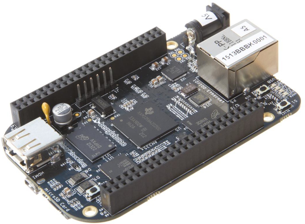
This document is the System Reference Manual for the BeagleBone Black and covers its use and design. The board will primarily be referred to in the remainder of this document simply as the board, although it may also be referred to as the BeagleBone Black as a reminder. There are also references to the original BeagleBone as well, and will be referenced as simply BeagleBone.

This design is subject to change without notice as we will work to keep improving the design as the product matures based on feedback and experience. Software updates will be frequent and will be independent of the hardware revisions and as such not result in a change in the revision number.

Make sure you check the support Wiki frequently for the most up to date information.

Change History

This section describes the change history of this document and board. Document changes are not always a result of a board change. A board change will always result in a document change.

imageimageREF: BBONEBLK_SRM BeagleBone Black System Rev C.1

___________________ *Reference Manual * ___________________ [[document-change-history]] Document Change History +++++++++++++++++++++++ _________________________________________ [[_bookmark5]]**Table 1. Change History** _________________________________________ [cols=",,,",options="header",] |======================================================================= a| _____ *Rev* _____ a| _________ *Changes* _________ a| ______ *Date* ______ a| ____ *By* ____ a| __ A4 __ a| ___________ Preliminary ___________ a| _______________ January 4, 2013 _______________ a| __ GC __ a| __ A5 __ a| __________________ Production release __________________ a| ______________ January 8.2013 ______________ a| __ GC __ a| ____ A5.1 ____ a| 1. ________________________________________________________________ Added information on Power button and the battery access points. ________________________________________________________________ 2. __________________________________ Final production released version. __________________________________ a| ____________ April 1 2013 ____________ a| __ GC __ a| ____ A5.2 ____ a| 1. _______________ Edited version. _______________ 2. _____________________________________________ Added numerous pictures of the Rev A5A board. _____________________________________________ a| _____________ April 23 2013 _____________ a| __ GC __ a| ____ A5.3 ____ a| 1. ________________________________ Updated serial number locations. ________________________________ 2. _______________________________________ Corrected the feature table for 4 UARTS _______________________________________ 3. _____________________________________________________________ Corrected eMMC pin table to match other tables in the manual. _____________________________________________________________ a| ______________ April 30, 2013 ______________ a| __ GC __ a| ____ A5.4 ____ a| 1. __________________________________________________________________________________ Corrected revision listed in section 2. Rev A5A is the initial production release. __________________________________________________________________________________ 2. _____________________________________________ Added all the locations of the serial numbers _____________________________________________ 3. _________________________________________ Made additions to the compatibility list. _________________________________________ 4. ____________________________________ Corrected Table 7 for LED GPIO pins. ____________________________________ 5. ____________________ Fixed several typos. ____________________ 6. _______________________________________________________________________ Added some additional information about LDOs and Step- Down converters. _______________________________________________________________________ 7. ____________________________ Added short section on HDMI. ____________________________ a| ____________ May 12, 2013 ____________ a| __ GC __ a| ____ A5.5 ____ a| 1. ___________________________ Release of the A5B version. ___________________________ 2. _______________________________________________ The LEDS were dimmed by changing the resistors. _______________________________________________ 3. __________________________________________________________ The serial termination mode was incorporated into the PCB. __________________________________________________________ a| ____________ May 20, 2013 ____________ a| __ GC __ a| ____ A5.6 ____ a| 1. ____________________________ Added information on Rev A5C ____________________________ 2. _______________________________________________ Added PRU/ICSS options to tables for P8 and P9. _______________________________________________ 3. _________________________ Added section on USB Host _________________________ 4. __________________________ Correct modes on Table 15. __________________________ 5. _________________ Fixed a few typos _________________ a| _____________ June 16, 2013 _____________ a| __ GC __ a| ____ A5.7 ____ a| 1. ________________________________ Updated assembly revision to A6. ________________________________ 2. _____________________________________________________________________________ PCB change to add buffer to the reset line and ground the oscillator GND pin. _____________________________________________________________________________ 3. _____________________________________________________________ Added resistor on PCB for connection of OSC_GND to board GND. _____________________________________________________________ a| ______________ August 9, 2013 ______________ a| __ GC __ a| __ A6 __ a| _________________________ \1. Added Rev A6 changes. _________________________ a| ________________ October 11, 2013 ________________ a| __ GC __ a| ___ A6A ___ a| _________________________ \1. Added Rev A6A changes _________________________ a| _________________ December 17, 2013 _________________ a| __ GC __ a| _ B _ a| ___________________________________________ \1. Changed the processor to the AM3358BZCZ ___________________________________________ a| ________________ January 20, 2013 ________________ a| __ GC __ a| _ C _ a| 1. _________________________________ Changed the eMMC from 2GB to 4GB. _________________________________ 2. ___________________________________________ Added additional supplier to DDR2 and eMMC. ___________________________________________ a| _____________ March 21,2014 _____________ a| __ GC __ a| ___ C.1 ___ a| ___________________________________________________________ \1. Added note to recommend powering off the board with the power button. ___________________________________________________________ a| _____________ March 22.2014 _____________ a| __ GC __ |======================================================================= [[ref-bboneblk_srm-beaglebone-black-system-rev-c.1-9]] image:media2/media/image1.png[image,width=194,height=34]image:media2/media/image2.jpeg[image,width=172,height=27]REF: BBONEBLK_SRM BeagleBone Black System Rev C.1

*Reference Manual *

  1. Board Changes

1. [[_bookmark7]][[bookmark7]]**Rev C** * Changed the eMMC from 2GB to 4GB. ______________________________________________________________________________________________________________________________________________________________________________________________________________ 2GB devices are getting harder to get as they are being phased out. This required us to move to 4GB. We now have two sources for the device. This will however, require an increase in the price of the board. ______________________________________________________________________________________________________________________________________________________________________________________________________________ 1. [[_bookmark8]][[bookmark8]]**Rev B** * Changed the processor to the AM3358BZCZ100. 1. [[_bookmark9]][[bookmark9]]**Rev A6A** ** Added connection from 32KHz OSC_GND to system ground and changed C106 to 1uF. ** Changes C25 to 2.2uF. This resolved an issue we were seeing in a few boards where the board would not boot in 1 in 20 tries. ** Change required PCB revision to B6. 2. [[_bookmark10]][[bookmark10]]**Rev A6** ** In random instances there could be a glitch in the SYS_RESETn signal from the processor where the SYS_RESETn signal was taken high for a momentary amount of time before it was supposed to. To prevent this, the signal was ORed with the PORZn (Power On reset). ** Noise issues were observed in other design where the clock oscillator was getting hit due to a suspected issue in ground bounce. A zero ohm resistor was added to connect the OSC_GND to the system ground. _____________________________________________________________ There are no new features added as a result of these changes. _____________________________________________________________ 1. [[_bookmark11]][[bookmark11]]**Rev A5C** ____________________________________________________________________________________________________________________________________________________________________________________________________________________________________________________ We were seeing some fallout in production test where we were seeing some jitter on the HDMI display test. It started showing up on out second production run. R46, R47, R48 were changed to 0 ohm from 33 ohm. R45 was taken from 330 ohm to 22 ohm. We do not know of any boards that were shipped with this issue as this issue was caught in production test. No impact on features or functionality resulted from this change. ____________________________________________________________________________________________________________________________________________________________________________________________________________________________________________________ [[ref-bboneblk_srm-beaglebone-black-system-rev-c.1-10]] image:media2/media/image1.png[image,width=194,height=34]image:media2/media/image2.jpeg[image,width=172,height=27]REF: BBONEBLK_SRM BeagleBone Black System Rev C.1 ++++++++++++++++++++++++++++++++++++++++++++++++++++++++++++++++++++++++++++++++++++++++++++++++++++++++++++++++++++++++++++++++++++++++++++++++++++++++++++++++++ ___________________ *Reference Manual * ___________________ 1. [[_bookmark12]][[bookmark12]]**Rev A5B** _______________________________________________________________________________________________________________________ There is no operational difference between the Rev A5A and the Rev A5B. There were two changes made to the A5B version. _______________________________________________________________________________________________________________________ * Due to complaints about the brightness of the LEDs keeping people awake at night, the LEDs were dimmed. Resistors were changed from 820 ohms to 4.75K ohms. * The PCB revision was updated to incorporate the hand mod that was being done on the board during manufacturing. The resistor was incorporated into the next revision of the PCB. _________________________________________________________________________________________________________________________________________________________________________________________ The highest supported resolution is now listed as 1920x1080@24Hz. This was not a result of any hardware changes but only updated software. The A5A version also supports this resolution. _________________________________________________________________________________________________________________________________________________________________________________________ 1. [[_bookmark13]][[bookmark13]]**Rev A5A** _________________________________________________________________________________________________________ This is the initial production release of the board. We will be tracking changes from this point forward. _________________________________________________________________________________________________________ [[ref-bboneblk_srm-beaglebone-black-system-rev-c.1-11]] image:media2/media/image1.png[image,width=194,height=34]image:media2/media/image2.jpeg[image,width=172,height=27]REF: BBONEBLK_SRM BeagleBone Black System Rev C.1 ++++++++++++++++++++++++++++++++++++++++++++++++++++++++++++++++++++++++++++++++++++++++++++++++++++++++++++++++++++++++++++++++++++++++++++++++++++++++++++++++++ ___________________ *Reference Manual * ___________________ [[connecting-up-your-beaglebone-black]] Connecting Up Your BeagleBone Black ^^^^^^^^^^^^^^^^^^^^^^^^^^^^^^^^^^^ _________________________________________________________________________________________________ This section provides instructions on how to hook up your board. Two scenarios will be discussed: _________________________________________________________________________________________________ 1. Tethered to a PC and 2. As a standalone development platform in a desktop PC configuration. [[whats-in-the-box]] What’s In the Box +++++++++++++++++ _________________________________________________________________ In the box you will find three main items as shown in *Figure 1*. _________________________________________________________________ * BeagleBone Black * miniUSB to USB Type A Cable * Instruction card with link to the support WIKI address. _________________________________________________________________________________________________________________________________________________________ This is sufficient for the tethered scenario and creates an out of box experience where the board can be used immediately with no other equipment needed. _________________________________________________________________________________________________________________________________________________________ image:media2/media/image4.jpeg[image,width=564,height=399] _______________________________________ [[_bookmark16]]**Figure 1. In The Box** _______________________________________ [[ref-bboneblk_srm-beaglebone-black-system-rev-c.1-12]] image:media2/media/image1.png[image,width=194,height=34]image:media2/media/image2.jpeg[image,width=172,height=27]REF: BBONEBLK_SRM BeagleBone Black System Rev C.1 ++++++++++++++++++++++++++++++++++++++++++++++++++++++++++++++++++++++++++++++++++++++++++++++++++++++++++++++++++++++++++++++++++++++++++++++++++++++++++++++++++ ___________________ *Reference Manual * ___________________ [[main-connection-scenarios]] Main Connection Scenarios +++++++++++++++++++++++++ __________________________________________________________________________________________________________________________________________________________________________________________________________________________________________________________________________________________________________________________________________________________________________________________________________________________________ This section will describe how to connect the board for use. This section is basically a slightly more detailed description of the Quick Start Guide that came in the box. There is also a Quick Start Guide document on the board that should also be referred to. The intent here is that someone looking t purchase the board will be able to read this section and get a good idea as to what the initial set up will be like. The board can be configured in several different ways, but we will discuss the two most common scenarios as described in the Quick Start Guide card that comes in the box. __________________________________________________________________________________________________________________________________________________________________________________________________________________________________________________________________________________________________________________________________________________________________________________________________________________________________ * Tethered to a PC via the USB cable ** Board is accessed as a storage drive ** Or a RNDIS Ethernet connection. * Standalone desktop ** Display ** Keyboard and mouse ** External 5V power supply ___________________________________________________________________________________________________________________________________________________________________________________________________________________________ Each of these configurations is discussed in general terms in the following sections. For an up-to-date list of confirmed working accessories please go to http://circuitco.com/support/index.php?title=BeagleBone_Black_Accessories[_http://circuitco.com/support/index.php?title=BeagleBone_Black_Accessories_] ___________________________________________________________________________________________________________________________________________________________________________________________________________________________ [[tethered-to-a-pc]] Tethered To A PC ++++++++++++++++ ______________________________________________________________________________________________________________________________________________________________________________________________________________________________________________________________________________________________________________________ In this configuration, the board is powered by the PC via the provided USB cable--no other cables are required. The board is accessed either as a USB storage drive or via the browser on the PC. You need to use either Firefox or Chrome on the PC, IEx will not work properly. *Figure 2* shows this configuration. ______________________________________________________________________________________________________________________________________________________________________________________________________________________________________________________________________________________________________________________ image:media2/media/image5.jpeg[image,width=626,height=166] ___________________________________________________ [[_bookmark19]]**Figure 2. Tethered Configuration** ___________________________________________________ [[ref-bboneblk_srm-beaglebone-black-system-rev-c.1-13]] image:media2/media/image1.png[image,width=194,height=34]image:media2/media/image2.jpeg[image,width=172,height=27]REF: BBONEBLK_SRM BeagleBone Black System Rev C.1 ++++++++++++++++++++++++++++++++++++++++++++++++++++++++++++++++++++++++++++++++++++++++++++++++++++++++++++++++++++++++++++++++++++++++++++++++++++++++++++++++++ ______________________________________________________________________________________________________________________________________________________________________________________________________________________________________________________ *Reference Manual * All the power for the board is provided by the PC via the USB cable. In some instances, the PC may not be able to supply sufficient power for the board. In that case, an external 5VDC power supply can be used, but this should rarely be necessary. ______________________________________________________________________________________________________________________________________________________________________________________________________________________________________________________ 1. [[_bookmark20]][[bookmark20]]**Connect the Cable to the Board** 1. Connect the small connector on the USB cable to the board as shown in *Figure 4*. The connector is on the bottom side of the board. image:media2/media/image6.jpeg[image,width=450,height=206] ________________________________________________________ [[_bookmark21]]**Figure 3. USB Connection to the Board** ________________________________________________________ 1. Connect the large connector of the USB cable to your PC or laptop USB port. 2. The board will power on and the power LED will be on as shown in *Figure 4* ______ below. ______ image:media2/media/image7.jpeg[image,width=399,height=256] ____________________________________________ [[_bookmark22]]**Figure 4. Board Power LED** ____________________________________________ [[ref-bboneblk_srm-beaglebone-black-system-rev-c.1-14]] image:media2/media/image1.png[image,width=194,height=34]image:media2/media/image2.jpeg[image,width=172,height=27]REF: BBONEBLK_SRM BeagleBone Black System Rev C.1 ++++++++++++++++++++++++++++++++++++++++++++++++++++++++++++++++++++++++++++++++++++++++++++++++++++++++++++++++++++++++++++++++++++++++++++++++++++++++++++++++++ ___________________ *Reference Manual * ___________________ 1. When the board starts to the booting process started by the process of applying power, the LEDs will come on in sequence as shown in *Figure 5* below. It will take a few seconds for the status LEDs to come on, so be patient. The LEDs will be flashing in an erratic manner as it begins to boot the Linux kernel. image:media2/media/image8.jpeg[image,width=538,height=245] ______________________________________________ [[_bookmark23]]**Figure 5. Board Boot Status** ______________________________________________ 1. [[_bookmark24]][[bookmark24]]**Accessing the Board as a Storage Drive** ________________________________________________________________________________________________________________________________________________________________________________________________________________________________________________________________ The board will appear around a USB Storage drive on your PC after the kernel has booted, which will take a round 10 seconds. The kernel on the board needs to boot before the port gets enumerated. Once the board appears as a storage drive, do the following: ________________________________________________________________________________________________________________________________________________________________________________________________________________________________________________________________ 1. Open the USB Drive folder. 2. Click on the file named *start.html* 3. The file will be opened by your browser on the PC and you should get a display showing the Quick Start Guide. 4. Your board is now operational! Follow the instructions on your PC screen. [[ref-bboneblk_srm-beaglebone-black-system-rev-c.1-15]] image:media2/media/image1.png[image,width=194,height=34]image:media2/media/image2.jpeg[image,width=172,height=27]REF: BBONEBLK_SRM BeagleBone Black System Rev C.1 ++++++++++++++++++++++++++++++++++++++++++++++++++++++++++++++++++++++++++++++++++++++++++++++++++++++++++++++++++++++++++++++++++++++++++++++++++++++++++++++++++ ___________________ *Reference Manual * ___________________ [[standalone-wdisplay-and-keyboardmouse]] Standalone w/Display and Keyboard/Mouse +++++++++++++++++++++++++++++++++++++++ ____________________________________________________________________________________________________________________________________________________________________________________________________________________________________________________________________________________________________________________________________________ In this configuration, the board works more like a PC, totally free from any connection to a PC as shown in *Figure 6*. It allows you to create your code to make the board do whatever you need it to do. It will however require certain common PC accessories. These accessories and instructions are described in the following section. ____________________________________________________________________________________________________________________________________________________________________________________________________________________________________________________________________________________________________________________________________________ image:media2/media/image9.jpeg[image,width=353,height=402] _________________________________________________________________ [[_bookmark26]]**Figure 6. Desktop Configuration** Optionally an Ethernet cable can also be used for network access. _________________________________________________________________ 1. [[_bookmark27]][[bookmark27]]**Required Accessories** _________________________________________________________________________________________ In order to use the board in this configuration, you will need the following accessories: _________________________________________________________________________________________ * \(1) 5VDC 1A power supply * \(1) HDMI monitor or a DVI-D monitor. (*NOTE:* Only HDMI will give you audio capability). * \(1) Micro HDMI to HDMI cable or a Micro HDMI to DVI-D adapter. * \(1) USB wireless keyboard and mouse combo. * \(1) USB HUB (OPTIONAL). The board has only one USB host port, so you may need to use a USB Hub if your keyboard and mouse requires two ports. [[ref-bboneblk_srm-beaglebone-black-system-rev-c.1-16]] image:media2/media/image1.png[image,width=194,height=34]image:media2/media/image2.jpeg[image,width=172,height=27]REF: BBONEBLK_SRM BeagleBone Black System Rev C.1 ++++++++++++++++++++++++++++++++++++++++++++++++++++++++++++++++++++++++++++++++++++++++++++++++++++++++++++++++++++++++++++++++++++++++++++++++++++++++++++++++++ ___________________________________________________________________________________________________________________________________________________________________________________________________________________________ *Reference Manual * For an up-to-date list of confirmed working accessories please go to http://circuitco.com/support/index.php?title=BeagleBone_Black_Accessories[_http://circuitco.com/support/index.php?title=BeagleBone_Black_Accessories_] ___________________________________________________________________________________________________________________________________________________________________________________________________________________________ 1. [[_bookmark28]][[bookmark28]]**Connecting Up the Board** 1. Connect the big end of the HDMI cable as shown in *Figure 7* to your HDMI monitor. Refer to your monitor Owner’s Manual for the location of your HDMI port. If you have a DVI-D Monitor go to *Step 3*, otherwise proceed to *Step 4.* image:media2/media/image10.jpeg[image,width=251,height=88] ___________________________________________________________________ [[_bookmark29]]**Figure 7. Connect microHDMI Cable to the Monitor** ___________________________________________________________________ 1. If you have a DVI-D monitor you must use a DVI-D to HDMI adapter in addition to your HDMI cable. An example is shown in *Figure 8* below from two perspectives. If you use this configuration, you will not have audio support. ____________________________________________________ image:media2/media/image11.jpeg[image]To the Monitor [[_bookmark30]]**Figure 8. DVI-D to HDMI Adapter** ____________________________________________________ 1. If you have a single wireless keyboard and mouse combination such as seen in Figure *9* below, you need to plug the receiver in the USB host port of the board as shown in *Figure 10*. [[ref-bboneblk_srm-beaglebone-black-system-rev-c.1-17]] image:media2/media/image1.png[image,width=194,height=34]image:media2/media/image2.jpeg[image,width=172,height=27]REF: BBONEBLK_SRM BeagleBone Black System Rev C.1 ++++++++++++++++++++++++++++++++++++++++++++++++++++++++++++++++++++++++++++++++++++++++++++++++++++++++++++++++++++++++++++++++++++++++++++++++++++++++++++++++++ ___________________ *Reference Manual * ___________________ image:media2/media/image12.jpeg[image,width=236,height=108] [[_bookmark31]]**Figure 9. Wireless Keyboard and Mouse Combo** ___________________________________________________________ image:media2/media/image13.jpeg[image,width=266,height=221] ___________________________________________________________ [[_bookmark32]]**Figure 10. Connect Keyboard and Mouse Receiver to the Board** __________________________________________________________________________________________________________________________________________________________________________________________________________________________________________________________________________________________________________ If you have a wired USB keyboard requiring two USB ports, you will need a HUB similar to the ones shown in *Figure 11*. You may want to have more than one port for other devices. Note that the board can only supply up to 500mA, so if you plan to load it down, it will need to be externally powered. __________________________________________________________________________________________________________________________________________________________________________________________________________________________________________________________________________________________________________ image:media2/media/image14.jpeg[image] _____________________________________________________ [[_bookmark33]]**Figure 11. Keyboard and Mouse Hubs** _____________________________________________________ 1. Connect the Ethernet Cable ___________________________________________________________________________________________________________________________________________________________________________________________________________________ If you decide you want to connect to your local area network, an Ethernet cable can be used. Connect the Ethernet Cable to the Ethernet port as shown in *Figure 12*. Any standard 100M Ethernet cable should work. ___________________________________________________________________________________________________________________________________________________________________________________________________________________ [[ref-bboneblk_srm-beaglebone-black-system-rev-c.1-18]] image:media2/media/image1.png[image,width=194,height=34]image:media2/media/image2.jpeg[image,width=172,height=27]REF: BBONEBLK_SRM BeagleBone Black System Rev C.1 ++++++++++++++++++++++++++++++++++++++++++++++++++++++++++++++++++++++++++++++++++++++++++++++++++++++++++++++++++++++++++++++++++++++++++++++++++++++++++++++++++ ___________________ *Reference Manual * ___________________ image:media2/media/image17.jpeg[image,width=431,height=256] _______________________________________________________ [[_bookmark34]]**Figure 12. Ethernet Cable Connection** _______________________________________________________ 1. [[_bookmark35]][[bookmark35]]**Apply Power** _________________________________________________________________________________ The final step is to plug in the DC power supply to the DC power jack as shown in *Figure 13* below. image:media2/media/image18.jpeg[image,width=618,height=298] [[_bookmark36]]**Figure 13. External DC Power** _________________________________________________________________________________ 1. The cable needed to connect to your display is a microHDMI to HDMI. Connect the microHDMI connector end to the board at this time. The connector is on the bottom side of the board as shown in *Figure 14* below. [[ref-bboneblk_srm-beaglebone-black-system-rev-c.1-19]] image:media2/media/image1.png[image,width=194,height=34]image:media2/media/image2.jpeg[image,width=172,height=27]REF: BBONEBLK_SRM BeagleBone Black System Rev C.1 ++++++++++++++++++++++++++++++++++++++++++++++++++++++++++++++++++++++++++++++++++++++++++++++++++++++++++++++++++++++++++++++++++++++++++++++++++++++++++++++++++ ___________________ *Reference Manual * ___________________ image:media2/media/image19.jpeg[image,width=540,height=227] ____________________________________________________________________________________________________________________________________________________________________________ [[_bookmark37]]**Figure 14. Connect microHDMI Cable to the Board** The connector is fairly robust, but we suggest that you not use the cable as a leash for your Beagle. Take proper care not to put too much stress on the connector or cable. ____________________________________________________________________________________________________________________________________________________________________________ 1. Booting the Board _________________________________________________________________________________________________________________________________________________________________________________________________________________________________________________________________________________________________________________________________________ As soon as the power is applied to the board, it will start the booting up process. When the board starts to boot the LEDs will come on in sequence as shown in *Figure 15* below. It will take a few seconds for the status LEDs to come on, so be patient. The LEDs will be flashing in an erratic manner as it boots the Linux kernel. _________________________________________________________________________________________________________________________________________________________________________________________________________________________________________________________________________________________________________________________________________ image:media2/media/image8.jpeg[image,width=538,height=245] ______________________________________________________________________________________________________________________________________________________________________________ [[_bookmark38]]**Figure 15. Board Boot Status** While the four user LEDS can be over written and used as desired, they do have specific meanings in the image that is shipped with the board once the Linux kernel has booted. ______________________________________________________________________________________________________________________________________________________________________________ [[ref-bboneblk_srm-beaglebone-black-system-rev-c.1-20]] image:media2/media/image1.png[image,width=194,height=34]image:media2/media/image2.jpeg[image,width=172,height=27]REF: BBONEBLK_SRM BeagleBone Black System Rev C.1 ++++++++++++++++++++++++++++++++++++++++++++++++++++++++++++++++++++++++++++++++++++++++++++++++++++++++++++++++++++++++++++++++++++++++++++++++++++++++++++++++++ ___________________ *Reference Manual * ___________________ * *USER0* is the heartbeat indicator from the Linux kernel. * *USER1* turns on when the microSD card is being accessed * *USER2* is an activity indicator. It turns on when the kernel is not in the idle loop. * *USER3* turns on when the onboard eMMC is being accessed. 1. A Booted System 1. The board will have a mouse pointer appear on the screen as it enters the Linux boot step. You may have to move the physical mouse to get the mouse pointer to appear. The system can come up in the suspend mode with the HDMI port in a sleep mode. 2. After a minute or two a login screen will appear. You do not have to do anything at this point. 3. After a minute or two the desktop will appear. It should be similar to the one shown in *Figure 16*. HOWEVER, it will change from one release to the next, so do not expect your system to look exactly like the one in the figure, but it will be very similar. 4. And at this point you are ready to go! *Figure 16* shows the desktop after booting. image:media2/media/image20.jpeg[image,width=511,height=288] ____________________________________________ [[_bookmark39]]**Figure 16. Desktop Screen** \8. Powering Down ____________________________________________ 1. Press the power button momentarily 2. The system will power down automatically. 3. Remove the power jack. [[ref-bboneblk_srm-beaglebone-black-system-rev-c.1-21]] image:media2/media/image1.png[image,width=194,height=34]image:media2/media/image2.jpeg[image,width=172,height=27]REF: BBONEBLK_SRM BeagleBone Black System Rev C.1 ++++++++++++++++++++++++++++++++++++++++++++++++++++++++++++++++++++++++++++++++++++++++++++++++++++++++++++++++++++++++++++++++++++++++++++++++++++++++++++++++++ ___________________ *Reference Manual * ___________________ [[beaglebone-black-overview]] BeagleBone Black Overview ^^^^^^^^^^^^^^^^^^^^^^^^^ ______________________________________________________________________________________________________________________________________________________________________________________________________________________________________________________________________________________________________________________________________________________________________________________________________________________________________________________________________________________________________________________________________________________________ The BeagleBone Black is the latest addition to the BeagleBoard.org family and like its predecessors, is designed to address the Open Source Community, early adopters, and anyone interested in a low cost ARM Cortex-A8 based processor. It has been equipped with a minimum set of features to allow the user to experience the power of the processor and is not intended as a full development platform as many of the features and interfaces supplied by the processor are not accessible from the BeagleBone Black via onboard support of some interfaces. It is not a complete product designed to do any particular function. It is a foundation for experimentation and learning how to program the processor and to access the peripherals by the creation of your own software and hardware. It also offers access to many of the interfaces and allows for the use of add-on boards called capes, to add many different combinations of features. A user may also develop their own board or add their own circuitry. BeagleBone Black is manufactured and warranted by Circuitco LLC in Richardson Texas for the benefit of the community and its supporters. In addition, Circuitco provides the RMA support for the BeagleBone Black. Jason Kridner of Texas Instruments handles the community promotions and is the spokesman for BeagleBoard.org. The board is designed by Gerald Coley, an employee of Texas Instruments and a charter member of the BeagleBoard.org community. The PCB layout was done by Circuitco and Circuitco is the sole funder of its development and transition to production. The Software is written and supported by the thousands of community members, including Jason Kridner, employees of Texas Instruments, DigiKey, and Circuitco. . ______________________________________________________________________________________________________________________________________________________________________________________________________________________________________________________________________________________________________________________________________________________________________________________________________________________________________________________________________________________________________________________________________________________________ [[ref-bboneblk_srm-beaglebone-black-system-rev-c.1-22]] image:media2/media/image1.png[image,width=194,height=34]image:media2/media/image2.jpeg[image,width=172,height=27]REF: BBONEBLK_SRM BeagleBone Black System Rev C.1 ++++++++++++++++++++++++++++++++++++++++++++++++++++++++++++++++++++++++++++++++++++++++++++++++++++++++++++++++++++++++++++++++++++++++++++++++++++++++++++++++++ ___________________ *Reference Manual * ___________________ [[beaglebone-compatibility]] BeagleBone Compatibility ++++++++++++++++++++++++ _____________________________________________________________________________________________________________________________________________________________________________________________________________________________________________________ The board is intended to be compatible with the original BeagleBone as much as possible. There are several areas where there are differences between the two designs. These differences are listed below, along with the reasons for the differences. _____________________________________________________________________________________________________________________________________________________________________________________________________________________________________________________ * Sitara AM3358BZCZ100, 1GHZ, processor. ** Sorry, we just had to make it faster. * 512MB DDR3L ** _Cost reduction_ ** Performance boost ** Memory size increase ** Lower power * No Serial port by default. ** _Cost reduction_ ** Can be added by buying a TTL to USB Cable that is widely available ** Single largest cost reduction action taken * No JTAG emulation over USB. ** _Cost reduction._ JTAG header is not populated, but can easily be mounted. * EEPROM Reduced from 32KB to 4KB ** Cost Reduction * Onboard Managed NAND (eMMC) ** 4GB ** _Cost reduction_ ** Performance boost x8 vs. x4 bits ** Performance boost due to deterministic properties vs. microSD card * GPMC bus may not be accessible from the expansion headers in some cases ** Result of eMMC on the main board ** Signals are still routed to the expansion connector ** If eMMC is not used, signals can be used via expansion if eMMC is held in reset * There may be 10 less GPIO pins available ** Result of eMMC ** If eMMC is not used, could still be used * The power expansion header, for battery and backlight, has been removed ** __Cost reduction, s__pace reduction ** Four pins were added to provide access to the battery charger function. * HDMI interface onboard ** Feature addition ** Audio and video capable ** Micro HDMI * No three function USB cable ** _Cost reduction_ * GPIO3_21 has a 24.576 MHZ clock on it. [[ref-bboneblk_srm-beaglebone-black-system-rev-c.1-23]] image:media2/media/image1.png[image,width=194,height=34]image:media2/media/image2.jpeg[image,width=172,height=27]REF: BBONEBLK_SRM BeagleBone Black System Rev C.1 ++++++++++++++++++++++++++++++++++++++++++++++++++++++++++++++++++++++++++++++++++++++++++++++++++++++++++++++++++++++++++++++++++++++++++++++++++++++++++++++++++ ___________________ *Reference Manual * ___________________ * This is required by the HDMI Framer for Audio purposes. We needed to run a clock into the processor to generate the correct clock frequency. The pin on the processor was already routed to the expansion header. In order not to remove this feature on the expansion header, it was left connected. In order to use the pin as a GPIO pin, you need to disable the clock. While this disables audio to the HDMI, the fact that you want to use this pin for something else, does the same thing. [[ref-bboneblk_srm-beaglebone-black-system-rev-c.1-24]] image:media2/media/image1.png[image,width=194,height=34]image:media2/media/image2.jpeg[image,width=172,height=27]REF: BBONEBLK_SRM BeagleBone Black System Rev C.1 ++++++++++++++++++++++++++++++++++++++++++++++++++++++++++++++++++++++++++++++++++++++++++++++++++++++++++++++++++++++++++++++++++++++++++++++++++++++++++++++++++ ___________________ *Reference Manual * ___________________ [[beaglebone-black-features-and-specification]] BeagleBone Black Features and Specification +++++++++++++++++++++++++++++++++++++++++++ _____________________________________________________________________________________________________________________________________________________________________ This section covers the specifications and features of the board and provides a high level description of the major components and interfaces that make up the board. *Table 2* provides a list of the features. [[_bookmark43]]**Table 2. BeagleBone Black Features** _____________________________________________________________________________________________________________________________________________________________________ [cols=",",options="header",] |======================================================================= | a| _________ *Feature* _________ a| ___________ *Processor* ___________ a| ____________________ Sitara AM3358BZCZ100 1GHz, 2000 MIPS ____________________ a| _________________ *Graphics Engine* _________________ a| _________________________ SGX530 3D, 20M Polygons/S _________________________ a| ______________ *SDRAM Memory* ______________ a| __________________ 512MB DDR3L 800MHZ __________________ a| _______________ *Onboard Flash* _______________ a| ______________________ 4GB, 8bit Embedded MMC ______________________ a| ______ *PMIC* ______ a| ________________________________________________ TPS65217C PMIC regulator and one additional LDO. ________________________________________________ a| _______________ *Debug Support* _______________ a| _______________________________________________ Optional Onboard 20-pin CTI JTAG, Serial Header _______________________________________________ a| ______________ *Power Source* ______________ a| _________________ miniUSB USB or DC Jack _________________ a| ___________________________ 5VDC External Via Expansion Header ___________________________ a| _____ *PCB* _____ a| ___________ 3.4” x 2.1” ___________ a| ________ 6 layers ________ a| ____________ *Indicators* ____________ a| _____________________________________________ 1-Power, 2-Ethernet, 4-User Controllable LEDs _____________________________________________ a| ________________________ *HS USB 2.0 Client Port* ________________________ a| _______________________________________ Access to USB0, Client mode via miniUSB _______________________________________ a| ______________________ *HS USB 2.0 Host Port* ______________________ a| _____________________________________________ Access to USB1, Type A Socket, 500mA LS/FS/HS _____________________________________________ a| _____________ *Serial Port* _____________ a| ___________________________________________________________ UART0 access via 6 pin 3.3V TTL Header. Header is populated ___________________________________________________________ a| __________ *Ethernet* __________ a| ____________ 10/100, RJ45 ____________ a| __________________ *SD/MMC Connector* __________________ a| ______________ microSD , 3.3V ______________ a| ____________ *User Input* ____________ a| ________________________ Reset Button Boot Button Power Button ________________________ a| ___________ *Video Out* ___________ a| __________________________________________ 16b HDMI, 1280x1024 (MAX) 1024x768,1280x720,1440x900 ,1920x1080@24Hz w/EDID Support __________________________________________ a| _______ *Audio* _______ a| __________________________ Via HDMI Interface, Stereo __________________________ a| ______________________ *Expansion Connectors* ______________________ a| _____________________________________________________________________________________ Power 5V, 3.3V , VDD_ADC(1.8V) 3.3V I/O on all signals McASP0, SPI1, I2C, GPIO(69 max), LCD, GPMC, MMC1, MMC2, 7 AIN**_(1.8V MAX)_**, 4 Timers, 4 Serial Ports, CAN0, EHRPWM(0,2),XDMA Interrupt, Power button, Expansion Board ID (Up to 4 can be stacked) _____________________________________________________________________________________ a| ________ *Weight* ________ a| ____________________ 1.4 oz (39.68 grams) ____________________ a| _______ *Power* _______ a| ______________________ Refer to Section 6.1.7 ______________________ |======================================================================= [[ref-bboneblk_srm-beaglebone-black-system-rev-c.1-25]] image:media2/media/image1.png[image,width=194,height=34]image:media2/media/image2.jpeg[image,width=172,height=27]REF: BBONEBLK_SRM BeagleBone Black System Rev C.1 ++++++++++++++++++++++++++++++++++++++++++++++++++++++++++++++++++++++++++++++++++++++++++++++++++++++++++++++++++++++++++++++++++++++++++++++++++++++++++++++++++ ___________________ *Reference Manual * ___________________ [[board-component-locations]] Board Component Locations +++++++++++++++++++++++++ ______________________________________________________________________________________________________________________________________________________________________________ This section describes the key components on the board. It provides information on their location and function. Familiarize yourself with the various components on the board. ______________________________________________________________________________________________________________________________________________________________________________ 1. [[_bookmark45]][[bookmark45]]**Connectors, LEDs, and Switches** ________________________________________________________________________________________________________________________________________________________________________ image:media2/media/image21.jpeg[image,width=492,height=323]**Figure 17** below shows the locations of the connectors, LEDs, and switches on the PCB layout of the board. [[_bookmark46]]**Figure 17. Connectors, LEDs and Switches** ________________________________________________________________________________________________________________________________________________________________________ * *DC Power* is the main DC input that accepts 5V power. * *Power Button* alerts the processor to initiate the power down sequence and is used to power down the board. * *10/100 Ethernet* is the connection to the LAN. * *Serial Debug* is the serial debug port. * *USB Client* is a miniUSB connection to a PC that can also power the board. * *BOOT switch* can be used to force a boot from the microSD card if the power is cycled on the board, removing power and reapplying the power to the board.. * There are four blue **LED**S that can be used by the user. * *Reset Button* allows the user to reset the processor. * *microSD* slot is where a microSD card can be installed. * *microHDMI* connector is where the display is connected to. * *USB Host* can be connected different USB interfaces such as Wi-Fi, BT, Keyboard, etc. [[ref-bboneblk_srm-beaglebone-black-system-rev-c.1-26]] image:media2/media/image1.png[image,width=194,height=34]image:media2/media/image2.jpeg[image,width=172,height=27]REF: BBONEBLK_SRM BeagleBone Black System Rev C.1 ++++++++++++++++++++++++++++++++++++++++++++++++++++++++++++++++++++++++++++++++++++++++++++++++++++++++++++++++++++++++++++++++++++++++++++++++++++++++++++++++++ ___________________ *Reference Manual * ___________________ 1. [[_bookmark47]][[bookmark47]]**Key Components** ___________________________________________________________________________________________ *Figure 18* below shows the locations of the key components on the PCB layout of the board. ___________________________________________________________________________________________ image:media2/media/image22.jpeg[image,width=578,height=419] ____________________________________________ [[_bookmark48]]**Figure 18. Key Components** ____________________________________________ * *Sitara AM3358BZCZ100* is the processor for the board. * *Micron 512MB DDR3L* or *Kingston 512mB DDR3* is the Dual Data Rate RAM memory. * *TPS65217C PMIC* provides the power rails to the various components on the board. * *SMSC Ethernet PHY* is the physical interface to the network. * *Micron eMMC* is an onboard MMC chip that holds up to 4GB of data. * *HDMI* Framer provides control for an HDMI or DVI-D display with an adapter. [[ref-bboneblk_srm-beaglebone-black-system-rev-c.1-27]] image:media2/media/image1.png[image,width=194,height=34]image:media2/media/image2.jpeg[image,width=172,height=27]REF: BBONEBLK_SRM BeagleBone Black System Rev C.1 ++++++++++++++++++++++++++++++++++++++++++++++++++++++++++++++++++++++++++++++++++++++++++++++++++++++++++++++++++++++++++++++++++++++++++++++++++++++++++++++++++ ___________________ *Reference Manual * ___________________ [[beaglebone-black-high-level-specification]] BeagleBone Black High Level Specification ^^^^^^^^^^^^^^^^^^^^^^^^^^^^^^^^^^^^^^^^^ ___________________________________________________________________________ This section provides the high level specification of the BeagleBone Black. ___________________________________________________________________________ [[block-diagram]] Block Diagram

Figure 19 below is the high level block diagram of the BeagleBone Black.

image

Figure 19. BeagleBone Black Key Components

Processor

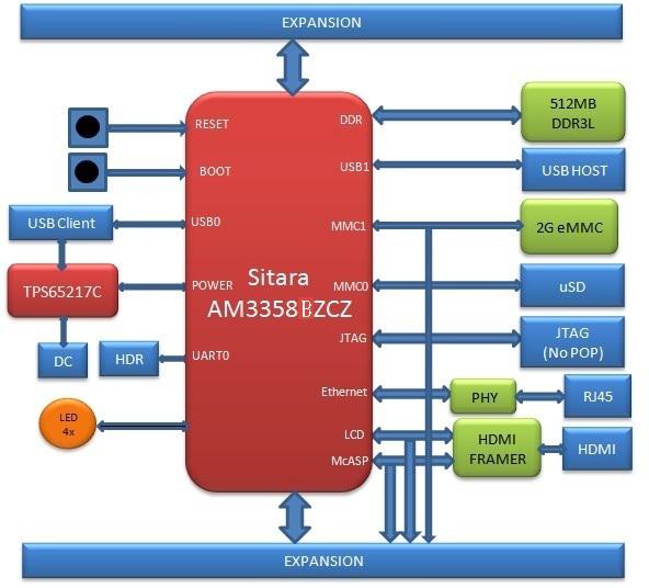
The revision B board has moved to the Sitara AM3358BZCZ100 device.

imageimageREF: BBONEBLK_SRM BeagleBone Black System Rev C.1

___________________ *Reference Manual * ___________________ [[memory]] Memory ++++++ ____________________________________________________________________________________ Described in the following sections are the three memory devices found on the board. ____________________________________________________________________________________ 1. [[_bookmark54]][[bookmark54]]**512MB DDR3L** _____________________________________________________________________________________________________ A single 256Mb x16 DDR3L 4Gb (512MB) memory device is used. The memory used is is one of two devices: _____________________________________________________________________________________________________ * MT41K256M16HA-125 from Micron * D2516EC4BXGGB from Kingston ____________________________________________________________________________________________________________________________________________________ It will operate at a clock frequency of 400MHz yielding an effective rate of 800MHZ on the DDR3L bus allowing for 1.6GB/S of DDR3L memory bandwidth. ____________________________________________________________________________________________________________________________________________________ 1. [[_bookmark55]][[bookmark55]]**4KB EEPROM** ______________________________________________________________________________________________________________________________________________________________________________________________________________________________________________________________________________________________________________________________________________________________________________________________________ A single 4KB EEPROM is provided on I2C0 that holds the board information. This information includes board name, serial number, and revision information. This is the not the same as the one used on the original BeagleBone. The device was changed for cost reduction reasons. It has a test point to allow the device to be programmed and otherwise to provide write protection when not grounded. ______________________________________________________________________________________________________________________________________________________________________________________________________________________________________________________________________________________________________________________________________________________________________________________________________ 1. [[_bookmark56]][[bookmark56]]**4GB Embedded MMC** ____________________________________________________________________________________________________________________________________________________________________________________________________________________________________________________________________________________________________________________________________________________________________________________________________________________________________________________________________________________________________________________________________________________________________________________________________________________________________________________________________ A single 4GB embedded MMC (eMMC) device is on the board. The device connects to the MMC1 port of the processor, allowing for 8bit wide access. Default boot mode for the board will be MMC1 with an option to change it to MMC0, the SD card slot, for booting from the SD card as a result of removing and reapplying the power to the board. Simply pressing the reset button will not change the boot mode. MMC0 cannot be used in 8Bit mode because the lower data pins are located on the pins used by the Ethernet port. This does not interfere with SD card operation but it does make it unsuitable for use as an eMMC port if the 8 bit feature is needed. ____________________________________________________________________________________________________________________________________________________________________________________________________________________________________________________________________________________________________________________________________________________________________________________________________________________________________________________________________________________________________________________________________________________________________________________________________________________________________________________________________ 1. [[_bookmark57]][[bookmark57]]**MicroSD Connector** __________________________________________________________________________________________________________________________________________________________________________________________________________________________________________________________________________________________________________________________________________________________________________________________________________________ The board is equipped with a single microSD connector to act as the secondary boot source for the board and, if selected as such, can be the primary boot source. The connector will support larger capacity microSD cards. The microSD card is not provided with the board. Booting from MMC0 will be used to flash the eMMC in the production environment or can be used by the user to update the SW as needed. __________________________________________________________________________________________________________________________________________________________________________________________________________________________________________________________________________________________________________________________________________________________________________________________________________________ 1. [[_bookmark58]][[bookmark58]]**Boot Modes** ________________________________________________ As mentioned earlier, there are four boot modes: ________________________________________________ [[ref-bboneblk_srm-beaglebone-black-system-rev-c.1-29]] image:media2/media/image1.png[image,width=194,height=34]image:media2/media/image2.jpeg[image,width=172,height=27]REF: BBONEBLK_SRM BeagleBone Black System Rev C.1

*Reference Manual *

  • eMMC Boot…This is the default boot mode and will allow for the fastest boot time and will enable the board to boot out of the box using the pre-flashed OS image without having to purchase an microSD card or an microSD card writer.

  • SD Boot…This mode will boot from the microSD slot. This mode can be used to override what is on the eMMC device and can be used to program the eMMC when used in the manufacturing process or for field updates.

  • Serial Boot…This mode will use the serial port to allow downloading of the software direct. A separate USB to serial cable is required to use this port.

  • USB Boot…This mode supports booting over the USB port.

Software to support USB and serial boot modes is not provided by beagleboard.org.

Please contact TI for support of this feature.

A switch is provided to allow switching between the modes.

  • Holding the boot switch down during a removal and reapplication of power without a microSD card inserted will force the boot source to be the USB port and if nothing is detected on the USB client port, it will go to the serial port for download.

  • Without holding the switch, the board will boot try to boot from the eMMC. If it is empty, then it will try booting from the microSD slot, followed by the serial port, and then the USB port.

  • If you hold the boot switch down during the removal and reapplication of power to the board, and you have a microSD card inserted with a bootable image, the board will boot from the microSD card.

NOTE: Pressing the RESET button on the board will NOT result in a change of the boot mode. You MUST remove power and reapply power to change the boot mode. The boot pins are sampled during power on reset from the PMIC to the processor. The reset button on the board is a warm reset only and will not force a boot mode change.

Power Management

The TPS65217C power management device is used along with a separate LDO to provide power to the system. The TPS65217C version provides for the proper voltages required for the DDR3L. This is the same device as used on the original BeagleBone with the exception of the power rail configuration settings which will be changed in the internal EEPROM to the TPS65217C to support the new voltages.

DDR3L requires 1.5V instead of 1.8V on the DDR2 as is the case on the original BeagleBone. The 1.8V regulator setting has been changed to 1.5V for the DDR3L. The

imageimageREF: BBONEBLK_SRM BeagleBone Black System Rev C.1

____________________________________________________________________________________________________________________________________________________________________________________________________________________ *Reference Manual * LDO3 3.3V rail has been changed to 1.8V to support those rails on the processor. LDO4 is still 3.3V for the 3.3V rails on the processor. An external *LDOTLV70233* provides the 3.3V rail for the rest of the board. ____________________________________________________________________________________________________________________________________________________________________________________________________________________ [[pc-usb-interface]] PC USB Interface ++++++++++++++++ ______________________________________________________________________________________________________________________________________________ The board has a miniUSB connector that connects the USB0 port to the processor. This is the same connector as used on the original BeagleBone. ______________________________________________________________________________________________________________________________________________ [[serial-debug-port]] Serial Debug Port +++++++++++++++++ __________________________________________________________________________________________________________________________________________________________________________________________________________________________________________________________________________________________________________________________________________________________ Serial debug is provided via UART0 on the processor via a single 1x6 pin header. In order to use the interface a USB to TTL adapter will be required. The header is compatible with the one provided by FTDI and can be purchased for about $12 to $20 from various sources. Signals supported are TX and RX. None of the handshake signals are supported. __________________________________________________________________________________________________________________________________________________________________________________________________________________________________________________________________________________________________________________________________________________________ [[usb1-host-port]] USB1 Host Port ++++++++++++++ __________________________________________________________________________________________________________________________________________________________________________________________________________________________________________________________________________________________________________________________________________________________________________________________________ On the board is a single USB Type A female connector with full LS/FS/HS Host support that connects to USB1 on the processor. The port can provide power on/off control and up to 500mA of current at 5V. Under USB power, the board will not be able to supply the full 500mA, but should be sufficient to supply enough current for a lower power USB device supplying power between 50 to 100mA. You can use a wireless keyboard/mouse configuration or you can add a HUB for standard keyboard and mouse interfacing. __________________________________________________________________________________________________________________________________________________________________________________________________________________________________________________________________________________________________________________________________________________________________________________________________ [[power-sources]] Power Sources +++++++++++++ _____________________________________________________ The board can be powered from four different sources: _____________________________________________________ * A USB port on a PC * A 5VDC 1A power supply plugged into the DC connector. * A power supply with a USB connector. * Expansion connectors ____________________________________________________________________________________________________________________________________________________________________________________________________________________________________________________________________________________________________________________________________________________ The USB cable is shipped with each board. This port is limited to 500mA by the Power Management IC. It is possible to change the settings in the *TPS65217C* to increase this current, but only after the initial boot. And, at that point the PC most likely will complain, but you can also use a dual connector USB cable to the PC to get to 1A. The power supply is not provided with the board but can be easily obtained from numerous sources. A 1A supply is sufficient to power the board, but if there is a cape ____________________________________________________________________________________________________________________________________________________________________________________________________________________________________________________________________________________________________________________________________________________ [[ref-bboneblk_srm-beaglebone-black-system-rev-c.1-31]] image:media2/media/image1.png[image,width=194,height=34]image:media2/media/image2.jpeg[image,width=172,height=27]REF: BBONEBLK_SRM BeagleBone Black System Rev C.1

*Reference Manual *

plugged into the board or you have a power hungry device or hub plugged into the host port, then more current may needed from the DC supply.

Power routed to the board via the expansion header could be provided from power derived on a cape. The DC supply should be well regulated and 5V +/-.25V.

Reset Button

When pressed and released, causes a reset of the board. The reset button used on the BeagleBone Black is a little larger than the one used on the original BeagleBone. It has also been moved out to the edge of the board so that it is more accessible.

Power Button

A power button is provided near the reset button close to the Ethernet connector. This button takes advantage of the input to the PMIC for power down features. While a lot of capes have a button, it was decided to add this feature to the board to ensure everyone had access to some new features. These features include:

  • Interrupt is sent to the processor to facilitate an orderly shutdown to save files and to un-mount drives.

  • Provides ability to let processor put board into a sleep mode to save power.

  • Can alert processor to wake up from sleep mode and restore state before sleep was entered.

If you hold the button down longer than 8 seconds, the board will power off if you release the button when the power LED turns off. If you continue to hold it, the board will power back up completing a power cycle.

We recommend that you use this method to power down the board. It will also help prevent contamination of the SD card or the eMMC.

If you do not remove the power jack, you can press the button again and the board will power up.

Indicators

There are a total of five blue LEDs on the board.

  • One blue power LED indicates that power is applied and the power management IC is up. If this LED flashes when applying power, it means that an excess current flow was detected and the PMIC has shut down.

  • Four blue LEDs that can be controlled via the SW by setting GPIO pins.

imageimageREF: BBONEBLK_SRM BeagleBone Black System Rev C.1

________________________________________________________________________________________________________________________________________________________________________________ *Reference Manual * In addition, there are two LEDs on the RJ45 to provide Ethernet status indication. One is yellow (100M Link up if on) and the other is green (Indicating traffic when flashing). ________________________________________________________________________________________________________________________________________________________________________________ [[cti-jtag-header]] CTI JTAG Header +++++++++++++++ _________________________________________________________________________________________________________________________________________________________________________________________________________________________________________________________________________________________ A place for an optional 20 pin CTI JTAG header is provided on the board to facilitate the SW development and debugging of the board by using various JTAG emulators. This header is not supplied standard on the board. To use this, a connector will need to be soldered onto the board. If you need the JTAG connector you can solder it on yourself. No other components are needed. The connector is made by Samtec and the part number is FTR-110-03-G-D-06. You can purchase it from http://www.digikey.com/[_www.digikey.com_.] _________________________________________________________________________________________________________________________________________________________________________________________________________________________________________________________________________________________ [[hdmi-interface]] HDMI Interface ++++++++++++++ __________________________________________________________________________________________________________________________________________________________________________________________________________________________________________________________________________________________________________________________________________________________________________________________________________________________________________________ A single HDMI interface is connected to the 16 bit LCD interface on the processor. The 16b interface was used to preserve as many expansion pins as possible to allow for use by the user. The NXP TDA19988BHN is used to convert the LCD interface to HDMI and convert the audio as well. The signals are still connected to the expansion headers to enable the use of LCD expansion boards or access to other functions on the board as needed. The HDMI device does not support HDCP copy protection. Support is provided via EDID to allow the SW to identify the compatible resolutions. Currently the following resolutions are supported via the software: __________________________________________________________________________________________________________________________________________________________________________________________________________________________________________________________________________________________________________________________________________________________________________________________________________________________________________________ * 1280 x 1024 * 1440 x 900 * 1024 x 768 * 1280 x 720 1. [[cape-board-support]] Cape Board Support ++++++++++++++++++ _______________________________________________________________________________________________________________________________________________________________________________________________________________________________________________________________________________________________________________________ The BeagleBone Black has the ability to accept up to four expansion boards or capes that can be stacked onto the expansion headers. The word cape comes from the shape of the board as it is fitted around the Ethernet connector on the main board. This notch acts as a key to ensure proper orientation of the cape. The majority of capes designed for the original BeagleBone will work on the BeagleBone Black. The two main expansion headers will be populated on the board. There are a few exceptions where certain capabilities may not be present or are limited to the BeagleBone Black. These include: _______________________________________________________________________________________________________________________________________________________________________________________________________________________________________________________________________________________________________________________ [[ref-bboneblk_srm-beaglebone-black-system-rev-c.1-33]] image:media2/media/image1.png[image,width=194,height=34]image:media2/media/image2.jpeg[image,width=172,height=27]REF: BBONEBLK_SRM BeagleBone Black System Rev C.1
Reference Manual
  • GPMC bus may NOT be available due to the use of those signals by the eMMC. If the eMMC is used for booting only and the file system is on the microSD card, then these signals could be used.

  • Another option is to use the microSD or serial boot modes and not use the eMMC.

  • The power expansion header is not on the BeagleBone Black so those functions are not supported.

For more information on cape support refer to Section 9.0.

imageimageREF: BBONEBLK_SRM BeagleBone Black System Rev C.1

___________________ *Reference Manual * ___________________ [[detailed-hardware-design]] Detailed Hardware Design ^^^^^^^^^^^^^^^^^^^^^^^^ ___________________________________________________________________________________________________________________________________________________________________________________________________________________________________________________ This section provides a detailed description of the Hardware design. This can be useful for interfacing, writing drivers, or using it to help modify specifics of your own design. *Figure 20* below is the high level block diagram of the board. For those who may be concerned, *Figure 20* is the same figure as *Figure 19* back on page 31**.** It is placed here again for convenience so it is closer to the topics to follow. ___________________________________________________________________________________________________________________________________________________________________________________________________________________________________________________ image:media2/media/image23.jpeg[image,width=504,height=455] ____________________________________________________________ [[_bookmark71]]**Figure 20. BeagleBone Black Block Diagram** ____________________________________________________________ [[ref-bboneblk_srm-beaglebone-black-system-rev-c.1-35]] image:media2/media/image1.png[image,width=194,height=34]image:media2/media/image2.jpeg[image,width=172,height=27]REF: BBONEBLK_SRM BeagleBone Black System Rev C.1

*Reference Manual *

Power Section

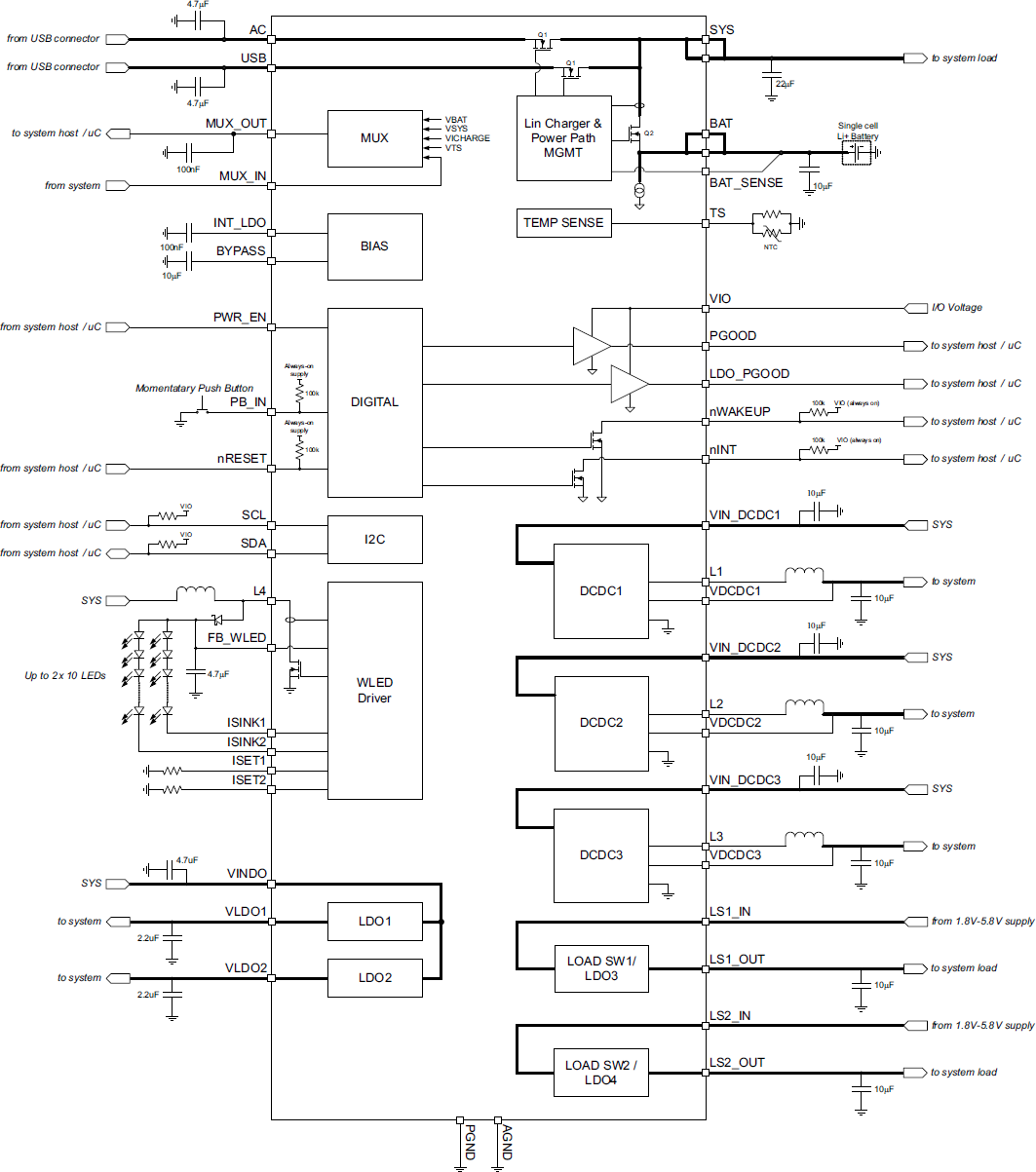
Figure 21 is the high level block diagram of the power section of the board.

image

Figure 21. High Level Power Block Diagram

This section describes the power section of the design and all the functions performed by the

TPS65217C.

  1. TPS65217C PMIC

The main Power Management IC (PMIC) in the system is the TPS65217C which is a single chip power management IC consisting of a linear dual-input power path, three step-down converters, and four LDOs. LDO stands for Low Drop Out. If you want to know more about an LDO, you can go to http://en.wikipedia.org/wiki/Low- dropout_regulator. If you want to learn more about step-down converters, you can go to http://en.wikipedia.org/wiki/DC-to-DC_converter

The system is supplied by a USB port or DC adapter. Three high-efficiency 2.25MHz step-down converters are targeted at providing the core voltage, MPU, and memory voltage for the board.

The step-down converters enter a low power mode at light load for maximum efficiency across the widest possible range of load currents. For low-noise applications the devices can be forced into fixed frequency PWM using the I2C interface. The step-down converters allow the use of small inductors and capacitors to achieve a small footprint solution size.

imageimageREF: BBONEBLK_SRM BeagleBone Black System Rev C.1

_____________________________________________________________________________________________________________________________________________________________________________________________________________________________________________________________________________________________________________________________________________________________________________________________________________________________________ *Reference Manual * LDO1 and LDO2 are intended to support system standby mode. In normal operation, they can support up to 100mA each. LDO3 and LDO4 can support up to 285mA each. By default only LDO1 is always ON but any rail can be configured to remain up in SLEEP state. In particular the DCDC converters can remain up in a low-power PFM mode to support processor suspend mode. The *TPS65217C* offers flexible power-up and power-down sequencing and several house-keeping functions such as power-good output, pushbutton monitor, hardware reset function and temperature sensor to protect the battery. For more information on the *TPS65217C*, refer to http://www.ti.com/product/tps65217C[_http://www.ti.com/product/tps65217C_]. _____________________________________________________________________________________________________________________________________________________________________________________________________________________________________________________________________________________________________________________________________________________________________________________________________________________________________ [[ref-bboneblk_srm-beaglebone-black-system-rev-c.1-37]] image:media2/media/image1.png[image,width=194,height=34]image:media2/media/image2.jpeg[image,width=172,height=27]REF: BBONEBLK_SRM BeagleBone Black System Rev C.1

*Reference Manual *

Figure 22 is the high level block diagram of the TPS65217C.

image

Figure 22. TPS65217C Block Diagram

imageimageREF: BBONEBLK_SRM BeagleBone Black System Rev C.1

___________________ *Reference Manual * ___________________ 1. [[_bookmark76]][[bookmark76]]**DC Input** _________________________________________________________________________ *Figure 23* below shows how the DC input is connected to the *TPS65217C*. _________________________________________________________________________ image:media2/media/image28.png[image] DGND DGND ______________________________________________________________________________________________________________________________________________________________________________________________________________________________________________________________________________________________________________________________________________________ [[_bookmark77]]**Figure 23. TPS65217 DC Connection** A 5VDC supply can be used to provide power to the board. The power supply current depends on how many and what type of add-on boards are connected to the board. For typical use, a 5VDC supply rated at 1A should be sufficient. If heavier use of the expansion headers or USB host port is expected, then a higher current supply will be required. The connector used is a 2.1MM center positive x 5.5mm outer barrel. The 5VDC rail is connected to the expansion header. It is possible to power the board via the expansion headers from an add-on card. The 5VDC is also available for use by the add-on cards when the power is supplied by the 5VDC jack on the board. ______________________________________________________________________________________________________________________________________________________________________________________________________________________________________________________________________________________________________________________________________________________ [[ref-bboneblk_srm-beaglebone-black-system-rev-c.1-39]] image:media2/media/image1.png[image,width=194,height=34]image:media2/media/image2.jpeg[image,width=172,height=27]REF: BBONEBLK_SRM BeagleBone Black System Rev C.1

*Reference Manual *

  1. USB Power

The board can also be powered from the USB port. A typical USB port is limited to 500mA max. When powering from the USB port, the VDD_5V rail is not provided to the expansion headers, so capes that require the 5V rail to supply the cape direct, bypassing the TPS65217C, will not have that rail available for use. The 5VDC supply from the USB port is provided on the SYS_5V, the one that comes from the TPS65217C, rail of the expansion header for use by a cape. Figure 24 is the connection of the USB power input on the PMIC.

U2

imageimageDGND

Figure 24. USB Power Connections

  1. Power Selection

The selection of either the 5VDC or the USB as the power source is handled internally to the TPS65217C and automatically switches to 5VDC power if both are connected. SW can change the power configuration via the I2C interface from the processor. In addition, the SW can read the TPS65217C and determine if the board is running on the 5VDC input or the USB input. This can be beneficial to know the capability of the board to supply current for things like operating frequency and expansion cards.

It is possible to power the board from the USB input and then connect the DC power supply. The board will switch over automatically to the DC input.

  1. Power Button

A power button is connected to the input of the TPS65217C. This is a momentary switch, the same type of switch used for reset and boot selection on the board.

If you push the button the TPS65217C will send an interrupt to the processor. It is up to the processor to then pull the PMIC_POWER_EN pin low at the correct time to power

imageimageREF: BBONEBLK_SRM BeagleBone Black System Rev C.1

_____________________________________________________________________________________________________________________________________________________________________________________________________________________________________________________________________________________________________________ *Reference Manual * down the board. At this point, the PMIC is still active, assuming that the power input was not removed. Pressing the power button will cause the board to power up again if the processor puts the board in the power off mode. In power off mode, the RTC rail is still active, keeping the RTC powered and running off the main power input. If you remove that power, then the RTC will not be powered. You also have the option of using the battery holes on the board to connect a battery if desired as discussed in the next section. If you push and hold the button for greater than 8 seconds, the PMIC will power down. But you must release the button when the power LED turns off. Holding the button past that point will cause the board to power cycle. _____________________________________________________________________________________________________________________________________________________________________________________________________________________________________________________________________________________________________________ 1. [[_bookmark82]][[bookmark82]]**Battery Access Pads** _______________________________________________________________________________________________________________________________________________________________________________________________________________________________________________________________________________________________ Four pads are provided on the board to allow access to the battery pins on the *TPS65217C*. The pads can be loaded with a 4x4 header or you may just wire a battery into the pads. In addition they could provide access via a cape if desired. The four signals are listed below in *Table 3*. [[_bookmark83]]**Table 3. BeagleBone Black Battery Pins** _______________________________________________________________________________________________________________________________________________________________________________________________________________________________________________________________________________________________ [cols=",,",options="header",] |========================================================== a| _____ *PIN* _____ a| _____________ *DESIGNATION* _____________ a| __________ *FUNCTION* __________ a| _____ *BAT* _____ a| ___ TP5 ___ a| _________________________ Battery connection point. _________________________ a| _______ *SENSE* _______ a| ___ TP6 ___ a| ___________________________________________________________ Battery voltage sense input, connect to BAT directly at the battery terminal. ___________________________________________________________ a| ____ *TS* ____ a| ___ TP7 ___ a| ___________________________________________________________ Temperature sense input. Connect to NTC thermistor to sense battery temperature. ___________________________________________________________ a| _____ *GND* _____ a| ___ TP8 ___ a| ______________ System ground. ______________ |========================================================== _________________________________________________________________________________________________________________________________________________________________________________________________________________________________________________________________________________________________ There is no fuel gauge function provided by the *TPS65217C*. That would need to be added if that function was required. If you want to add a fuel gauge, and option is to use 1-wire SPI or I2C device. You will need to add this using the expansion headers and place it on an expansion board. _________________________________________________________________________________________________________________________________________________________________________________________________________________________________________________________________________________________________ [[ref-bboneblk_srm-beaglebone-black-system-rev-c.1-41]] image:media2/media/image1.png[image,width=194,height=34]image:media2/media/image2.jpeg[image,width=172,height=27]REF: BBONEBLK_SRM BeagleBone Black System Rev C.1

*Reference Manual *

  1. Power Consumption

The power consumption of the board varies based on power scenarios and the board boot processes. Measurements were taken with the board in the following configuration:

  • DC powered and USB powered

  • HDMI monitor connected

  • USB HUB

  • 4GB Thumbdrive

  • Ethernet connected @ 100M

  • Serial debug cable connected

Table 4 is an analysis of the power consumption of the board in these various scenarios.

Table 4. BeagleBone Black Power Consumption(mA@5V)

MODE USB _ DC _ DC+USB

Reset


TBD _


TBD _


TBD _

Idling @ UBoot


210 _


210 _


210 _

Kernel Booting (Peak)


460 _


460 _


460 _

Kernel Idling


350 _


350 _


350 _

Kernel Idling Display Blank


280 _


280 _


280 _

Loading a Webpage


430 _


430 _


430 _

The current will fluctuate as various activates occur, such as the LEDs on and microSD/eMMC accesses.

  1. Processor Interfaces

The processor interacts with the TPS65217C via several different signals. Each of these signals is described below.

  1. *I2C0*

I2C0 is the control interface between the processor and the TPS65217C. It allows the processor to control the registers inside the TPS65217C for such things as voltage scaling and switching of the input rails.

  1. *PMC_POWR_EN*

On power up the VDD_RTC rail activates first. After the RTC circuitry in the processor has activated it instructs the TPS65217C to initiate a full power up cycle by activating the PMIC_POWR_EN signal by taking it HI. When powering down, the processor can take this pin low to start the power down process.

imageimageREF: BBONEBLK_SRM BeagleBone Black System Rev C.1

___________________ *Reference Manual * ___________________ 1. _*LDO_GOOD*_ _______________________________________________________________________________________________________________________________________________________________________________________________________________________________________________________________________________________________________________________________________________________________________________________________ This signal connects to the *RTC_PORZn* signal, RTC power on reset. The small “*n*” indicates that the signal is an active low signal. Word processors seem to be unable to put a bar over a word so the *n* is commonly used in electronics. As the RTC circuitry comes up first, this signal indicates that the LDOs, the 1.8V VRTC rail, is up and stable. This starts the power up process. _______________________________________________________________________________________________________________________________________________________________________________________________________________________________________________________________________________________________________________________________________________________________________________________________ 1. _*PMIC_PGOOD*_ _______________________________________________________________________________________ Once all the rails are up, the *PMIC_PGOOD* signal goes high. This releases the *PORZn* signal on the processor which was holding the processor reset. _______________________________________________________________________________________ 1. _*WAKEUP*_ ______________________________________________________________________________________________________________________________________________________________________________________________________________________________________________________________________________________ The WAKEUP signal from the *TPS65217C* is connected to the *EXT_WAKEUP* signal on the processor. This is used to wake up the processor when it is in a sleep mode. When an event is detected by the *TPS65217C,* such as the power button being pressed**,** it generates this signal. ______________________________________________________________________________________________________________________________________________________________________________________________________________________________________________________________________________________ 1. _*PMIC_INT*_ _________________________________________________________________________________________________________________________________________________________________________________________________________________________________________________________________________________________________ The *PMIC_INT* signal is an interrupt signal to the processor. Pressing the power button will send an interrupt to the processor allowing it to implement a power down mode in an orderly fashion, go into sleep mode, or cause it to wake up from a sleep mode. All of these require SW support. _________________________________________________________________________________________________________________________________________________________________________________________________________________________________________________________________________________________________ [[ref-bboneblk_srm-beaglebone-black-system-rev-c.1-43]] image:media2/media/image1.png[image,width=194,height=34]image:media2/media/image2.jpeg[image,width=172,height=27]REF: BBONEBLK_SRM BeagleBone Black System Rev C.1

*Reference Manual *

  1. Power Rails

Figure 25 shows the connections of each of the rails from the TPS65217C.

image

Figure 25. Power Rails

  1. *VRTC Rail*

The VRTC rail is a 1.8V rail that is the first rail to come up in the power sequencing. It provides power to the RTC domain on the processor and the I/O rail of the TPS65217C. It can deliver up to 250mA maximum.

  1. *VDD_3V3A Rail*

The VDD_3V3A rail is supplied by the TPS65217C and provides the 3.3V for the processor rails and can provide up to 400mA.

imageimageREF: BBONEBLK_SRM BeagleBone Black System Rev C.1

___________________ *Reference Manual * ___________________ 1. _*VDD_3V3B Rail*_ ____________________________________________________________________________________________________________________________________________________________________________________________________________________________________________ The current supplied by the *VDD_3V3A* rail is not sufficient to power all of the 3.3V rails on the board. So a second LDO is supplied, U4, a *TL5209A*, which sources the *VDD_3V3B* rail. It is powered up just after the *VDD_3V3A* rail. ____________________________________________________________________________________________________________________________________________________________________________________________________________________________________________ 1. _*VDD_1V8 Rail*_ ___________________________________________________________________________________________________________________________________________________________________________________________________ The *VDD_1V8* rail can deliver up to 400mA and provides the power required for the 1.8V rails on the processor and the HDMI framer. This rail is not accessible for use anywhere else on the board. ___________________________________________________________________________________________________________________________________________________________________________________________________ 1. _*VDD_CORE Rail*_ _____________________________________________________________________________________________________________________________________________________________________________________________________________________________________________________________________________________ The *VDD_CORE* rail can deliver up to 1.2A at 1.1V. This rail is not accessible for use anywhere else on the board and connects only to the processor. This rail is fixed at 1.1V and should not be adjusted by SW using the PMIC. If you do, then the processor will no longer work. _____________________________________________________________________________________________________________________________________________________________________________________________________________________________________________________________________________________ 1. _*VDD_MPU Rail*_ _______________________________________________________________________________________________________________________________________________________________________________________________________________________________________________________________________________________________________________ The *VDD_MPU* rail can deliver up to 1.2A. This rail is not accessible for use anywhere else on the board and connects only to the processor. This rail defaults to 1.1V and can be scaled up to allow for higher frequency operation. Changing of the voltage is set via the I2C interface from the processor. _______________________________________________________________________________________________________________________________________________________________________________________________________________________________________________________________________________________________________________ 1. _*VDDS_DDR Rail*_ _____________________________________________________________________________________________________________________________________________________________________________________________________________________________________________________________________ The *VDDS_DDR* rail defaults to *1.5V* to support the DDR3L rails and can deliver up to 1.2A. It is possible to adjust this voltage rail down to *1.35V* for lower power operation of the DDR3L device. Only DDR3L devices can support this voltage setting of 1.35V. _____________________________________________________________________________________________________________________________________________________________________________________________________________________________________________________________________ [[ref-bboneblk_srm-beaglebone-black-system-rev-c.1-45]] image:media2/media/image1.png[image,width=194,height=34]image:media2/media/image2.jpeg[image,width=172,height=27]REF: BBONEBLK_SRM BeagleBone Black System Rev C.1

*Reference Manual *

  1. *Power Sequencing*

The power up process is consists of several stages and events. Figure 26 describes the events that make up the power up process for the processer from the PMIC. This diagram is used elsewhere to convey additional information. I saw no need to bust it up into smaller diagrams. It is from the processor datasheet supplied by Texas Instruments.

image

Figure 26. Power Rail Power Up Sequencing

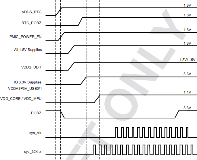
Figure 27 the voltage rail sequencing for the TPS65217C as it powers up and the voltages on each rail. The power sequencing starts at 15 and then goes to one. That is the way the TPS65217C is configured. You can refer to the TPS65217C datasheet for more information.

imageimageREF: BBONEBLK_SRM BeagleBone Black System Rev C.1

___________________ *Reference Manual * ___________________ image:media2/media/image39.png[image,width=221,height=185] [[_bookmark90]]**Figure 27. TPS65217C Power Sequencing Timing** 1. [[_bookmark91]][[bookmark91]]**Power LED** ________________________________________________________________________________________________________________________________________________________________________________________________________________________________________________________________________________________________________ The power LED is a blue LED that will turn on once the *TPS65217C* has finished the power up procedure. If you ever see the LED flash once, that means that the *TPS65217C* started the process and encountered an issue that caused it to shut down. The connection of the LED is shown in *Figure 25*. ________________________________________________________________________________________________________________________________________________________________________________________________________________________________________________________________________________________________________ 1. [[_bookmark92]][[bookmark92]]**TPS65217C Power Up Process** ________________________________________________________________________________________________________________________________________________________________ *Figure 28* shows the interface between the *TPS65217C* and the processor. It is a cut from the PDF form of the schematic and reflects what is on the schematic. ________________________________________________________________________________________________________________________________________________________________ image:media2/media/image40.png[image,width=556,height=162] [[_bookmark93]]**Figure 28. Power Processor Interfaces** ________________________________________________________________________________________________________________________________________________________________________________________________________________________________________________________ When voltage is applied, DC or USB, the *TPS65217C* connects the power to the SYS output pin which drives the switchers and LDOs in the *TPS65217C*. At power up all switchers and LDOs are off except for the *VRTC LDO* (1.8V), which provides power to the VRTC rail and controls the *RTC_PORZn* input pin to the processor, which starts the power up process of the processor. Once the RTC rail powers ________________________________________________________________________________________________________________________________________________________________________________________________________________________________________________________ [[ref-bboneblk_srm-beaglebone-black-system-rev-c.1-47]] image:media2/media/image1.png[image,width=194,height=34]image:media2/media/image2.jpeg[image,width=172,height=27]REF: BBONEBLK_SRM BeagleBone Black System Rev C.1

*Reference Manual *

up, the RTC_PORZn pin, driven by the LDO_PGOOD signal from the TPS65217C, of the processor is released.

Once the RTC_PORZn reset is released, the processor starts the initialization process. After the RTC stabilizes, the processor launches the rest of the power up process by activating the PMIC_POWER_EN signal that is connected to the TPS65217C which starts the TPS65217C power up process.

The LDO_PGOOD signal is provided by the TPS65217C to the processor. As this signal is 1.8V from the TPS65217C by virtue of the TPS65217C VIO rail being set to 1.8V, and the RTC_PORZ signal on the processor is 3.3V, a voltage level shifter, U4, is used. Once the LDOs and switchers are up on the TPS65217C, this signal goes active releasing the processor. The LDOs on the TPS65217C are used to power the VRTC rail on the processor.

  1. Processor Control Interface

Figure 28 above shows two interfaces between the processor and the TPS65217C used for control after the power up sequence has completed.

The first is the I2C0 bus. This allows the processor to turn on and off rails and to set the voltage levels of each regulator to supports such things as voltage scaling.

The second is the interrupt signal. This allows the TPS65217C to alert the processor when there is an event, such as when the power button is pressed. The interrupt is an open drain output which makes it easy to interface to 3.3V of the processor.

  1. Low Power Mode Support

This section covers three general power down modes that are available. These modes are only described from a Hardware perspective as it relates to the HW design.

  1. *RTC Only*

In this mode all rails are turned off except the VDD_RTC. The processor will need to turn off all the rails to enter this mode. The VDD_RTC staying on will keep the RTC active and provide for the wakeup interfaces to be active to respond to a wake up event.

  1. *RTC Plus DDR*

In this mode all rails are turned off except the VDD_RTC and the VDDS_DDR, which powers the DDR3L memory. The processor will need to turn off all the rails to enter this mode. The VDD_RTC staying on will keep the RTC active and provide for the wakeup interfaces to be active to respond to a wake up event.

imageimageREF: BBONEBLK_SRM BeagleBone Black System Rev C.1

__________________________________________________________________________________________________________________________________________________________________________________________________________________________________________ *Reference Manual * The *VDDS_DDR* rail to the DDR3L is provided by the 1.5V rail of the *TPS65217C* and with *VDDS_DDR* active, the DDR3L can be placed in a self refresh mode by the processor prior to power down which allows the memory data to be saved. Currently, this feature is not included in the standard software release. The plan is to include it in future releases. __________________________________________________________________________________________________________________________________________________________________________________________________________________________________________ 1. _*Voltage Scaling*_ _______________________________________________________________________________________________________________________________________________________________________________________________________________________________________________________________________ For a mode where the lowest power is possible without going to sleep, this mode allows the voltage on the ARM processor to be lowered along with slowing the processor frequency down. The I2C0 bus is used to control the voltage scaling function in the *TPS65217C*. _______________________________________________________________________________________________________________________________________________________________________________________________________________________________________________________________________ [[sitara-am3358bzcz100-processor]] Sitara AM3358BZCZ100 Processor ++++++++++++++++++++++++++++++ ________________________________________________________________________________________________________________________________________________________ The board is designed to use the Sitara AM3358BZCZ100 processor in the 15 x 15 package. Earlier revisions of the board used the XM3359AZCZ100 processor. ________________________________________________________________________________________________________________________________________________________ 1. [[_bookmark97]][[bookmark97]]**Description** ______________________________________________________________________________________________________________________________________________________________________________ *Figure 29* is a high level block diagram of the processor. For more information on the processor, go to http://www.ti.com/product/am3358[_http://www.ti.com/product/am3358_.] ______________________________________________________________________________________________________________________________________________________________________________ [[ref-bboneblk_srm-beaglebone-black-system-rev-c.1-49]] image:media2/media/image1.png[image,width=194,height=34]image:media2/media/image2.jpeg[image,width=172,height=27]REF: BBONEBLK_SRM BeagleBone Black System Rev C.1

*Reference Manual *

image

Figure 29. Sitara AM3358BZCZ Block Diagram

.

imageimageREF: BBONEBLK_SRM BeagleBone Black System Rev C.1

___________________ *Reference Manual * ___________________ 1. [[_bookmark99]][[bookmark99]]**High Level Features** _______________________________________________________________________________ *Table 5* below shows a few of the high level features of the Sitara processor. [[_bookmark100]]**Table 5. Processor Features** _______________________________________________________________________________ [cols=",,,",options="header",] |======================================= a| _________________ Operating Systems _________________ a| ________________________________________ Linux, Android, Windows Embedded CE,QNX, ThreadX ________________________________________ a| ______ MMC/SD ______ |3 a| _____________ Standby Power _____________ a| ____ 7 mW ____ a| ___ CAN ___ |2 a| _______ ARM CPU _______ a| _______________ 1 ARM Cortex-A8 _______________ a| __________ UART (SCI) __________ |6 a| ______________ ARM MHz (Max.) ______________ a| ____________________ 275,500,600,800,1000 ____________________ a| ___ ADC ___ a| ___________ 8-ch 12-bit ___________ a| _______________ ARM MIPS (Max.) _______________ a| ______________ 1000,1200,2000 ______________ a| ________ PWM (Ch) ________ |3 a| ____________ Graphics Acceleration ____________ a| ____ 1 3D ____ a| ____ eCAP ____ |3 a| ______________ Other Hardware Acceleration ______________ a| _____________________________ 2 PRU-ICSS,Crypto Accelerator _____________________________ a| ____ eQEP ____ |3 a| ________________ On-Chip L1 Cache ________________ a| _____________________ 64 KB (ARM Cortex-A8) _____________________ a| ___ RTC ___ |1 a| ________________ On-Chip L2 Cache ________________ a| ___________________ 256 KB (ARM Cortex- A8) ___________________ a| ___ I2C ___ |3 a| _____________ Other On-Chip Memory _____________ a| ______ 128 KB ______ a| _____ McASP _____ |2 a| _______________ Display Options _______________ a| ___ LCD ___ a| ___ SPI ___ |2 a| ______________________ General Purpose Memory ______________________ a| _______________________ 1 16-bit (GPMC, NAND flash, NOR Flash, SRAM) _______________________ a| ________ DMA (Ch) ________ a| __________ 64-Ch EDMA __________ a| ____ DRAM ____ a| ________________________________________ 1 16-bit (LPDDR-400, DDR2-532, DDR3-400) ________________________________________ a| _____________ IO Supply (V) _____________ a| ______________ 1.8V(ADC),3.3V ______________ a| _________ USB Ports _________ |2 a| _______________________________ Operating Temperature Range (C) _______________________________ a| _________ -40 to 90 _________ |======================================= 1. [[_bookmark101]][[bookmark101]]**Documentation** ___________________________________________________________________________________________________________________________________________________________________________________________________________________________________________________________________________________ Full documentation for the processor can be found on the TI website at http://www.ti.com/product/am3358[_http://www.ti.com/product/am3358_] for the current processor used on the board. Make sure that you always use the latest datasheets and Technical Reference Manuals (TRM). ___________________________________________________________________________________________________________________________________________________________________________________________________________________________________________________________________________________ [[ref-bboneblk_srm-beaglebone-black-system-rev-c.1-51]] REF: BBONEBLK_SRM BeagleBone Black System Rev C.1 +++++++++++++++++++++++++++++++++++++++++++++++++ ___________________ *Reference Manual * ___________________ 1. [[_bookmark102]][[bookmark102]]**Crystal Circuitry** ______________________________________________________________ *Figure 30* is the crystal circuitry for the AM3358 processor. C21 ______________________________________________________________ image:media2/media/image42.png[image]DGND _________________________________________________ [[_bookmark103]]**Figure 30. Processor Crystals** _________________________________________________ image:media2/media/image1.png[image,width=194,height=34]image:media2/media/image2.jpeg[image,width=172,height=27] [[ref-bboneblk_srm-beaglebone-black-system-rev-c.1-52]] REF: BBONEBLK_SRM BeagleBone Black System Rev C.1 +++++++++++++++++++++++++++++++++++++++++++++++++ ___________________ *Reference Manual * ___________________ 1. [[_bookmark104]][[bookmark104]]**Reset Circuitry** _____________________________________________________________________________________________________________________________________________________________________________________________________________________________________________________________________________________________________________________________________________________________________________________ *Figure 31* is the board reset circuitry. The initial power on reset is generated by the *TPS65217C* power management IC. It also handles the reset for the Real Time Clock. The board reset is the SYS_RESETn signal. This is connected to the NRESET_INOUT pin of the processor. This pin can act as an input or an output. When the reset button is pressed, it sends a warm reset to the processor and to the system. On the revision A5D board, a change was made. On power up, the NRESET_INOUT signal can act as an output. In this instance it can cause the SYS_RESETn line to go high prematurely. In order to prevent this, the PORZn signal from the TPS65217C is connected to the SYS_RESETn line using an open drain buffer. These ensure that the line does not momentarily go high on power up. _____________________________________________________________________________________________________________________________________________________________________________________________________________________________________________________________________________________________________________________________________________________________________________________ VDD_3V3A image:media2/media/image43.png[image]1% ,10V S_RESETn ____ 9,11 ____ image:media2/media/image1.png[image,width=194,height=34]image:media2/media/image2.jpeg[image,width=172,height=27] ____________________________________________________ AM3359 [[_bookmark105]]**Figure 31. Board Reset Circuitry** This change is also in all revisions after A5D. ____________________________________________________ [[ref-bboneblk_srm-beaglebone-black-system-rev-c.1-53]] image:media2/media/image1.png[image,width=194,height=34]image:media2/media/image2.jpeg[image,width=172,height=27]REF: BBONEBLK_SRM BeagleBone Black System Rev C.1

*Reference Manual *

DDR3L Memory

The BeagleBone Black uses a single MT41K256M16HA-125 512MB DDR3L device from Micron that interfaces to the processor over 16 data lines, 16 address lines, and 14 control lines. On rev C we added the Kingston KE4CN2H5A-A58 device as a source for the DDR3L device.

The following sections provide more details on the design.

  1. Memory Device

The design supports the standard DDR3 and DDR3L x16 devices and is built using the DDR3L. A single x16 device is used on the board and there is no support for two x8 devices. The DDR3 devices work at 1.5V and the DDR3L devices can work down to 1.35V to achieve lower power. The DDR3L comes in a 96-BALL FBGA package with

0.8 mil pitch. Other standard DDR3 devices can also be supported, but the DDR3L is the lower power device and was chosen for its ability to work at 1.5V or 1.35V. The standard frequency that the DDR3L is run at on the board is 400MHZ.

  1. DDR3L Memory Design

Figure 32 is the schematic for the DDR3L memory device. Each of the groups of signals is described in the following lines.

Address Lines: Provide the row address for ACTIVATE commands, and the column address and auto pre-charge bit (A10) for READ/WRITE commands, to select one location out of the memory array in the respective bank. A10 sampled during a PRECHARGE command determines whether the PRECHARGE applies to one bank (A10 LOW, bank selected by BA[2:0]) or all banks (A10 HIGH). The address inputs also provide the op-code during a LOAD MODE command. Address inputs are referenced to VREFCA. A12/BC#: When enabled in the mode register (MR), A12 is sampled during READ and WRITE commands to determine whether burst chop (on-the-fly) will be performed (HIGH = BL8 or no burst chop, LOW = BC4 burst chop).

Bank Address Lines: BA[2:0] define the bank to which an ACTIVATE, READ, WRITE, or PRECHARGE command is being applied. BA[2:0] define which mode register (MR0, MR1, MR2, or MR3) is loaded during the LOAD MODE command. BA[2:0] are referenced to VREFCA.

CK and CK# Lines: are differential clock inputs. All address and control input signals are sampled on the crossing of the positive edge of CK and the negative edge of CK#. Output data strobe (DQS, DQS#) is referenced to the crossings of CK and CK#.

Clock Enable Line: CKE enables (registered HIGH) and disables (registered LOW) internal circuitry and clocks on the DRAM. The specific circuitry that is enabled/disabled is dependent upon the DDR3 SDRAM configuration and operating mode. Taking CKE

REF: BBONEBLK_SRM BeagleBone Black System Rev C.1

*Reference Manual *

LOW provides PRECHARGE power-down and SELF REFRESH operations (all banks idle) or active power-down (row active in any bank). CKE is synchronous for power- down entry and exit and for self refresh entry. CKE is asynchronous for self refresh exit. Input buffers (excluding CK, CK#, CKE, RESET#, and ODT) are disabled during power- down. Input buffers (excluding CKE and RESET#) are disabled during SELF REFRESH. CKE is referenced to VREFCA.

DGND VDDS_DDR

3 DDR_RESETn

3

R97

R96

image10K,1%

image1.5K,1%

U12

T2

RESET#

J7

N3 _DDR_A0 _

DDR_A[15..0] 3

DDR_CLK

3 DDR_CLKn

3

K7 CK

K9 CKn

A0 P7

A1 P3

_DDR_A1 _

_DDR_A2 _

DDR_CKE

3

L2 CKE

A2 N2

_DDR_A3 _

DDR_CSn

3 DDR_RASn

3 DDR_CASn

3 DDR_WEn 3 DDR_D[15..0]

3 DDR_DQS1

3 DDR_DQSN1

3 DDR_DQS0

3 DDR_DQSN0

J3 K3 L3

DDR_D0 E3

DDR_D1 F7

DDR_D2 F2

DDR_D3 F8

DDR_D4 H3

DDR_D5 H8

DDR_D6 G2

DDR_D7 H7

DDR_D8 D7

DDR_D9 C3

DDR_D10 C8

DDR_D11 C2

DDR_D12 A7

DDR_D13 A2

DDR_D14 B8

DDR_D15 A3

C7 B7

F3 G3

CSn RASn CASn

WEn

DQ0 DQ1 DQ2 DQ3 DQ4 DQ5 DQ6 DQ7 DQ8 DQ9 DQ10 DQ11 DQ12 DQ13 DQ14 DQ15

UDQS UDQSn

LDQS LDQSn

A3 A4 A5 A6 A7 A8 A9 A10 A11 A12 A13 A14 A15 BA0 BA1 BA2

ODT

VDD1 VDD2 VDD3 VDD4 VDD5 VDD6 VDD7 VDD8

P8 _DDR_A4 _

P2 _DDR_A5 _

R8 _DDR_A6 _

R2 _DDR_A7 _

T8 _DDR_A8 _

R3 _DDR_A9 _

L7 _DDR_A10 _

R7 _DDR_A11 _

N7 _DDR_A12 _

T3 _DDR_A13 _

T7 _DDR_A14 _

M7 _DDR_A15 _

M2 _DDR_BA0 _

N8 _DDR_BA1 _

M3 _DDR_BA2 _

K1 _DDR_ODT _

B2 VDDS_DDR

R9 K2 K8 N1 N9 R1 D9

DDR_ODT 3

DDR_BA[2..0] 3

3 DDR_DQM1

3 DDR_DQM0

D3 E7

VDDS_DDR A1

C1 C9 D2 E9 F1 H2 H9

J1 J9 L1 L9

DDR_VREF

UDM LDM

VDDQ1 VDDQ2 VDDQ3 VDDQ4 VDDQ5 VDDQ7 VDDQ8 VDDQ9 VDDQ10

NC1 NC2 NC3 NC4

VDD9

VSS1 VSS2 VSS3 VSS4 VSS5 VSS6 VSS7 VSS8 VSS9 VSS10 VSS11 VSS12

VSSQ1 VSSQ2 VSSQ3 VSSQ4 VSSQ5 VSSQ6

A9 B3

E1 G8 J2 J8 M1 M9 P1 P9 T1 T9

B1 B9 D1 D8 E2 E8 F9

DGND

imageVDDS_DDR R98

10K,1%

R100 10K,1%

C124

M8

VREF_CA

H1

VREF_DQ

VSSQ7

VSSQ8 VSSQ9

ZQ

G1 G9

L8 _ZQ R99 _

240E

C123

0.001uf ,50V

0.1uf ,6.3V

MT41K256M16HA -125:E

4Gb(512MB) DDR3L

DGND

DGND

DGND

imageimage

Figure 32. DDR3L Memory Design

Chip Select Line: CS# enables (registered LOW) and disables (registered HIGH) the command decoder. All commands are masked when CS# is registered HIGH. CS# provides for external rank selection on systems with multiple ranks. CS# is considered part of the command code. CS# is referenced to VREFCA.

imageimageREF: BBONEBLK_SRM BeagleBone Black System Rev C.1

___________________________________________________________________________________________________________________________________________________________________________________________________________________________________________________________________________________________________________________________________________________________________________________________________________ *Reference Manual * *Input Data Mask Line:* DM is an input mask signal for write data. Input data is masked when DM is sampled HIGH along with the input data during a write access. Although the DM ball is input-only, the DM loading is designed to match that of the DQ and DQS balls. DM is referenced to VREFDQ. *On-die Termination Line:* ODT enables (registered HIGH) and disables (registered LOW) termination resistance internal to the DDR3L SDRAM. When enabled in normal operation, ODT is only applied to each of the following balls: DQ[7:0], DQS, DQS#, and DM for the x8; DQ[3:0], DQS, DQS#, and DM for the x4. The ODT input is ignored if disabled via the LOAD MODE command. ODT is referenced to VREFCA. ___________________________________________________________________________________________________________________________________________________________________________________________________________________________________________________________________________________________________________________________________________________________________________________________________________ 1. [[_bookmark109]][[bookmark109]]**Power Rails** _________________________________________________________________________________ The *DDR3L* memory device and the DDR3 rails on the processor are supplied by the *TPS65217C*. Default voltage is 1.5V but can be scaled down to 1.35V if desired. _________________________________________________________________________________ 1. [[_bookmark110]][[bookmark110]]**VREF** ______________________________________________________________________________________________________________________________________________________________________________________________________________________________________________________________________ The *VREF* signal is generated from a voltage divider on the *VDDS_DDR* rail that powers the processor DDR rail and the DDR3L device itself. *Figure 33* below shows the configuration of this signal and the connection to the DDR3L memory device and the processor. ______________________________________________________________________________________________________________________________________________________________________________________________________________________________________________________________________ image:media2/media/image53.png[image,width=371,height=256] ________________________________________________ [[_bookmark111]]**Figure 33. DDR3L VREF Design** ________________________________________________ [[ref-bboneblk_srm-beaglebone-black-system-rev-c.1-56]] image:media2/media/image1.png[image,width=194,height=34]image:media2/media/image2.jpeg[image,width=172,height=27]REF: BBONEBLK_SRM BeagleBone Black System Rev C.1

*Reference Manual *

4GB eMMC Memory

The eMMC is a communication and mass data storage device that includes a Multi- MediaCard (MMC) interface, a NAND Flash component, and a controller on an advanced 11-signal bus, which is compliant with the MMC system specification. The nonvolatile eMMC draws no power to maintain stored data, delivers high performance across a wide range of operating temperatures, and resists shock and vibration disruption.

One of the issues faced with SD cards is that across the different brands and even within the same brand, performance can vary. Cards use different controllers and different memories, all of which can have bad locations that the controller handles. But the controllers may be optimized for reads or writes. You never know what you will be getting. This can lead to varying rates of performance. The eMMC card is a known controller and when coupled with the 8bit mode, 8 bits of data instead of 4, you get double the performance which should result in quicker boot times.

The following sections describe the design and device that is used on the board to implement this interface.

  1. eMMC Device

The device used is one of two different devices:

  • Micron MTFC4GLDEA 0M WT

  • Kingston KE4CN2H5A-A58

The package is a 153 ball WFBGA device on both devices.

REF: BBONEBLK_SRM BeagleBone Black System Rev C.1

*Reference Manual *

  1. eMMC Circuit Design

Figure 34 is the design of the eMMC circuitry. The eMMC device is connected to the MMC1 port on the processor. MMC0 is still used for the microSD card as is currently done on the original BeagleBone. The size of the eMMC supplied is now 4GB.

The device runs at 3.3V both internally and the external I/O rails. The VCCI is an internal voltage rail to the device. The manufacturer recommends that a 1uF capacitor be attached to this rail, but a 2.2uF was chosen to provide a little margin.

Pullup resistors are used to increase the rise time on the signals to compensate for any capacitance on the board.

VDD_3V3B

imageVDD_3V3B

U5A

U7

U13

imageA3

AM3358_ZCZ

T13

R162

0,1%,DNI

MEM_MNAND_2GB

imageimageFigure 34. eMMC Memory Design

The pins used by the eMMC1 in the boot mode are listed below in Table 6.

imageTable 6. eMMC Boot Pins

For eMMC devices the ROM will only support raw mode. The ROM Code reads out raw sectors from image or the booting file within the file system and boots from it. In raw mode the booting image can be located at one of the four consecutive locations in the main area: offset 0x0 / 0x20000 (128 KB) / 0x40000 (256 KB) / 0x60000 (384 KB). For this reason, a booting image shall not exceed 128KB in size. However it is possible to

imageimageREF: BBONEBLK_SRM BeagleBone Black System Rev C.1

____________________________________________________________________________________________________________________________________________________________________________________________________________________________________________________________________________________________________________________________________________________________________________________________________________________________________________________________________________________________________________________________________________________________________________________________________________ *Reference Manual * flash a device with an image greater than 128KB starting at one of the aforementioned locations. Therefore the ROM Code does not check the image size. The only drawback is that the image will cross the subsequent image boundary. The raw mode is detected by reading sectors #0, #256, #512, #768. The content of these sectors is then verified for presence of a TOC structure. In the case of a *GP Device*, a Configuration Header (CH) *must* be located in the first sector followed by a *GP header*. The CH might be void (only containing a CHSETTINGS item for which the Valid field is zero). The ROM only supports the 4-bit mode. After the initial boot, the switch can be made to 8-bit mode for increasing the overall performance of the eMMC interface. ____________________________________________________________________________________________________________________________________________________________________________________________________________________________________________________________________________________________________________________________________________________________________________________________________________________________________________________________________________________________________________________________________________________________________________________________________________ 1. [[_bookmark117]][[bookmark117]]Board ID EEPROM ____________________________________________________________________________________________________________________________________________________________________ The BeagleBone is equipped with a single 32Kbit(4KB) 24LC32AT-I/OT EEPROM to allow the SW to identify the board. *Table 7* below defined the contents of the EERPOM. [[_bookmark118]]**Table 7. EEPROM Contents** ____________________________________________________________________________________________________________________________________________________________________ [cols=",,",options="header",] |======================================================================= a| ______ *Name* ______ a| ______________ *Size (bytes)* ______________ a| __________ *Contents* __________ a| ________ *Header* ________ a| ___ *4* ___ a| ______________________ *0xAA, 0x55, 0x33, EE* ______________________ a| ____________ *Board Name* ____________ a| ___ *8* ___ a| ___________________________________ *Name for board in ASCII: A335BNLT* ___________________________________ a| _________ *Version* _________ a| ___ *4* ___ a| ________________________________________________________________________________________________________ *Hardware version code for board in ASCII:* *00A3 for Rev A3, 00A4 for Rev A4, 00A5 for Rev A5, 00A6 for Rev A6,00B0 for Rev B, and 00C0 for Rev C.* ________________________________________________________________________________________________________ a| _______________ *Serial Number* _______________ a| ____ *12* ____ a| ____________________________________________________________________________________ *Serial number of the board. This is a 12 character string which is:* *WWYY4P16nnnn* *where: WW = 2 digit week of the year of production YY = 2 digit year of production* *BBBK = BeagleBone Black nnnn = incrementing board number* ____________________________________________________________________________________ a| ______________________ *Configuration Option* ______________________ a| ____ *32* ____ a| ______________________________________________________ *Codes to show the configuration setup on this board.* *All FF* ______________________________________________________ a| ______ *RSVD* ______ a| ___ *6* ___ a| ___________________ *FF FF FF FF FF FF* ___________________ a| ______ *RSVD* ______ a| ___ *6* ___ a| ___________________ *FF FF FF FF FF FF* ___________________ a| ______ *RSVD* ______ a| ___ *6* ___ a| ___________________ *FF FF FF FF FF FF* ___________________ a| ___________ *Available* ___________ a| ______ *4018* ______ a| ___________________________________________________ *Available space for other non-volatile codes/data* ___________________________________________________ |======================================================================= _____________________________________________________________ *Figure 35* shows the new design on the EEPROM interface**.** _____________________________________________________________ [[ref-bboneblk_srm-beaglebone-black-system-rev-c.1-59]] REF: BBONEBLK_SRM BeagleBone Black System Rev C.1 +++++++++++++++++++++++++++++++++++++++++++++++++ ___________________ *Reference Manual * ___________________ image:media2/media/image62.png[image,width=471,height=176] _________________________________________________________________________________________________________________________________________________________________________________________________________________________________________________________________ [[_bookmark119]]**Figure 35. EEPROM Design Rev A5** The EEPROM is accessed by the processor using the I2C 0 bus. The *WP* pin is enabled by default. By grounding the test point, the write protection is removed. The first 48 locations should not be written to if you choose to use the extras storage space in the EEPROM for other purposes. If you do, it could prevent the board from booting properly as the SW uses this information to determine how to set up the board. _________________________________________________________________________________________________________________________________________________________________________________________________________________________________________________________________ [[micro-secure-digital]] Micro Secure Digital ++++++++++++++++++++ ____________________________________________________________________________________________________________________________________ The microSD connector on the board will support a microSD card that can be used for booting or file storage on the BeagleBone Black. ____________________________________________________________________________________________________________________________________ 1. [[_bookmark121]][[bookmark121]]**microSD Design** ______________________________________________________________________ *Figure 36* below is the design of the microSD interface on the board. VDD_3V3B image:media2/media/image63.png[image]C153 10uF,10V C154 0.1uf ,6.3V ______________________________________________________________________ image:media2/media/image67.png[image,height=16]DGND U5A F18 MMC0_DAT2 F17 __ P7 1 __ 1. DAT2 9 _________________ GND 10 DGND MMC0_DAT3 MMC0_CMD MMC0_CLK G18 G17 G16 _________________ 1. CD/DAT3 2. CMD 3. VDD 4. CLOCK 5. VSS GND1 11 CD 12 GND2 13 __________________________ GND3 14 GND4 SD_CD VDD_3V3B R157 10K,1% MMC0_DAT0 MMC0_DAT1 MMC0_SDCD AM3358_ZCZ G15 C15 DGND 8 DAT0 _*microSD*_ MOLEX 502570-001 __________________________ image:media2/media/image1.png[image,width=194,height=34]image:media2/media/image2.jpeg[image,width=172,height=27] _________________________________________________________________________________________________________________ [[_bookmark122]]**Figure 36. microSD Design** The signals *MMC0-3* are the data lines for the transfer of data between the processor and the microSD connector. _________________________________________________________________________________________________________________ [[ref-bboneblk_srm-beaglebone-black-system-rev-c.1-60]] REF: BBONEBLK_SRM BeagleBone Black System Rev C.1 +++++++++++++++++++++++++++++++++++++++++++++++++ _______________________________________________________________________________________________________________________________________________________________________________________________________________________________________________________________________________________________________________________________________________________________________________________________________________________________________________________ *Reference Manual * The *MMC0_CLK* signal clocks the data in and out of the microSD card. The *MMCO_CMD* signal indicates that a command versus data is being sent. There is no separate card detect pin in the microSD specification. It uses *MMCO_DAT3* for that function. However, most microSD connectors still supply a CD function on the connectors. In the BeagleBone Black design, this pin is connected to the *MMC0_SDCD* pin for use by the processor. You can also change the pin to *GPIO0_6*, which is able to wake up the processor from a sleep mode when an microSD card is inserted into the connector. Pullup resistors are provided on the signals to increase the rise times of the signals to overcome PCB capacitance. Power is provided from the *VDD_3V3B* rail and a 10uF capacitor is provided for filtering. _______________________________________________________________________________________________________________________________________________________________________________________________________________________________________________________________________________________________________________________________________________________________________________________________________________________________________________________ [[user-leds]] User LEDs +++++++++ ________________________________________________________________________________________________________________________________________________________ There are four user LEDs on the BeagleBone Black. These are connected to GPIO pins on the processor. *Figure 37* shows the interfaces for the user LEDs. image:media2/media/image68.png[image]SY S_5V image:media2/media/image73.png[image]R72 820,5% R73 820,5% R74 820,5% R71 820,5% ________________________________________________________________________________________________________________________________________________________ D2 LTST-C191TBKT USR0 ________________ D3 LTST-C191TBKT USR1 D4 LTST-C191TBKT USR2 D5 LTST-C191TBKT USR3 ________________ 1. USR0 ____________ Q1A 5 2 DMC56404 Q1B DMC56404 Q2A 2 DMC56404 Q2B 5 DMC56404 3 USR1 3 USR2 ____________ 1. USR3 ___________ R76 100K,1% DGND DGND R77 100K,1% DGND ___________ DGND ___________ R78 100K,1% DGND DGND R79 100K,1% DGND DGND ___________ image:media2/media/image1.png[image,width=194,height=34]image:media2/media/image2.jpeg[image,width=172,height=27] _____________________________________________________________________________ [[_bookmark124]]**Figure 37. User LEDs** Resistors R71-R74 were changed to 4.75K on the revision A5B board. *Table 8* shows the signals used to control the four LEDs from the processor. _____________________________________________________________________________ [[ref-bboneblk_srm-beaglebone-black-system-rev-c.1-61]] image:media2/media/image1.png[image,width=194,height=34]image:media2/media/image2.jpeg[image,width=172,height=27]REF: BBONEBLK_SRM BeagleBone Black System Rev C.1

*Reference Manual *

Table 8. User LED Control Signals/Pins

LED _ GPIO SIGNAL _ PROC PIN

USR0

GPIO1_21


V15 _

USR1

GPIO1_22


U15 _

USR2

GPIO1_23


T15 _

USR3

GPIO1_24


V16 _

A logic level of “1” will cause the LEDs to turn on.

Boot Configuration

The design supports two groups of boot options on the board. The user can switch between these modes via the Boot button. The primary boot source is the onboard eMMC device. By holding the Boot button, the user can force the board to boot from the microSD slot. This enables the eMMC to be overwritten when needed or to just boot an alternate image. The following sections describe how the boot configuration works.

In most applications, including those that use the provided demo distributions available from beagleboard.org, the processor-external boot code is composed of two stages. After the primary boot code in the processor ROM passes control, a secondary stage (secondary program loader — "SPL" or "MLO") takes over. The SPL stage initializes only the required devices to continue the boot process, and then control is transferred to the third stage "U-boot". Based on the settings of the boot pins, the ROM knows where to go and get the SPL and UBoot code. In the case of the BeagleBone Black, that is either eMMC or microSD based on the position of the boot switch.

  1. Boot Configuration Design

Figure 38 shows the circuitry that is involved in the boot configuration process. On power up, these pins are read by the processor to determine the boot order. S2 is used to change the level of one bit from HI to LO which changes the boot order.

imageimageREF: BBONEBLK_SRM BeagleBone Black System Rev C.1

______________________________________________________________________________________________________________________________________________________________________________________________________________________________________________________________________________________________________________________________________________________________________________________________________________________________ *Reference Manual * VDD_3V3A image:media2/media/image74.png[image]DGND [[_bookmark128]]**Figure 38. Processor Boot Configuration Design** It is possible to override these setting via the expansion headers. But be careful not to add too much load such that it could interfere with the operation of the HDMI interface or LCD panels. If you choose to override these settings, it is strongly recommended that you gate these signals with the *SYS_RESETn* signal. This ensures that after coming out of reset these signals are removed from the expansion pins. ______________________________________________________________________________________________________________________________________________________________________________________________________________________________________________________________________________________________________________________________________________________________________________________________________________________________ [[default-boot-options]] Default Boot Options ++++++++++++++++++++ __________________________________________________________________________________________________________________________ Based on the selected option found in *Figure 39* below, each of the boot sequences for each of the two settings is shown. __________________________________________________________________________________________________________________________ image:media2/media/image75.png[image,width=579,height=119] ___________________________________________________________ [[_bookmark130]]**Figure 39. Processor Boot Configuration** ___________________________________________________________ [[ref-bboneblk_srm-beaglebone-black-system-rev-c.1-63]] image:media2/media/image1.png[image,width=194,height=34]image:media2/media/image2.jpeg[image,width=172,height=27]REF: BBONEBLK_SRM BeagleBone Black System Rev C.1

*Reference Manual *

The first row in Figure 39 is the default setting. On boot, the processor will look for the eMMC on the MMC1 port first, followed by the microSD slot on MMC0, USB0 and UART0. In the event there is no microSD card and the eMMC is empty, UART0 or USB0 could be used as the board source.

If you have a microSD card from which you need to boot from, hold the boot button down. On boot, the processor will look for the SPIO0 port first, then microSD on the MMC0 port, followed by USB0 and UART0. In the event there is no microSD card and the eMMC is empty, USB0 or UART0 could be used as the board source.

10/100 Ethernet

The BeagleBone Black is equipped with a 10/100 Ethernet interface. It uses the same PHY as is used on the original BeagleBone. The design is described in the following sections.

  1. Ethernet Processor Interface

Figure 40 shows the connections between the processor and the PHY. The interface is in the MII mode of operation.

VDD_3V3B

QFN32_5X5MM_EP3P3MM

Figure 40. Ethernet Processor Interface

This is the same interface as is used on the BeagleBone. No changes were made in this design for the board.

imageimageREF: BBONEBLK_SRM BeagleBone Black System Rev C.1

___________________ *Reference Manual * ___________________ 1. [[_bookmark134]][[bookmark134]]**Ethernet Connector Interface** _________________________________________________________________________ The off board side of the PHY connections are shown in *Figure 41* below. _________________________________________________________________________ VDD_PHY A ___________________________________________________________________________________________________________ image:media2/media/image76.png[image]DGND DGND [[_bookmark135]]**Figure 41. Ethernet Connector Interface** This is the same interface as is used on the BeagleBone. No changes were made in this design for the board. ___________________________________________________________________________________________________________ [[ref-bboneblk_srm-beaglebone-black-system-rev-c.1-65]] REF: BBONEBLK_SRM BeagleBone Black System Rev C.1 +++++++++++++++++++++++++++++++++++++++++++++++++ ___________________ *Reference Manual * ___________________ 1. [[_bookmark136]][[bookmark136]]**Ethernet PHY Power, Reset, and Clocks** __________________________________________________________________________________________________________________________________________________________ *Figure 42* shows the power, reset, and lock connections to the *LAN8710A* PHY. Each of these areas is discussed in more detail in the following sections. VDD_PHY A __________________________________________________________________________________________________________________________________________________________ image:media2/media/image86.png[image]VDD_3V3B ______________ C131 C132 C133 0.1uf ,6.3V 1 2 0.1uf ,6.3V 10uF,10V C135 0.1uf ,6.3V ______________ 150OHM800mA __________ FB4 DGND DGND DGND PHY _VDDCR __________ 1. RMII1_REFCLK ______________________ DGND R__12__4 __1__0,1%,DNI C136 470pF,_6.3V_ C134 1uF,10V ______________________ DGND R131 100,1% _____________ REFCLKO 7 RXCLK/PHY AD1 U14 *LAN8710A* _____________ 3,11 _________________________ SY S_RESETn R140 0,1%,D__N__I 19 nRST R141 PHY _XTAL1 1M,1%,DNI PHY _XTAL2 R142 0,1% RCLKI5N XTAL1/CLKIN 4 _________________________ XTAL2 _____________ R143 10,1% Y3 PHY X 2 1 C142 30pF,50V _____________ 25.000MHz XTAL150SMD_125X196 __________________________________________________________________________________________________________________________ C143 30pF,50V DGND image:media2/media/image1.png[image,width=194,height=34]image:media2/media/image2.jpeg[image,width=172,height=27]DGND DGND [[_bookmark137]]**Figure 42. Ethernet PHY, Power, Reset, and Clocks** __________________________________________________________________________________________________________________________ 1. _*VDD_3V3B Rail*_ ________________________________________________________________________________________________________________________________________________________________________________________________________________________________________________________________________________________________________________________ The VDD_3V3B rail is the main power rail for the *LAN8710A*. It originates at the VD_3V3B regulator and is the primary rail that supports all of the peripherals on the board. This rail also supplies the VDDIO rails which set the voltage levels for all of the I/O signals between the processor and the *LAN8710A*. ________________________________________________________________________________________________________________________________________________________________________________________________________________________________________________________________________________________________________________________ 1. _*VDD_PHYA Rail*_ _________________________________________________________________________________________________________________________________________________________________________________________________________________________________________________________ A filtered version of VDD_3V3B rail is connected to the VDD rails of the LAN8710 and the termination resistors on the Ethernet signals. It is labeled as *VDD_PHYA*. The filtering inductor helps block transients that may be seen on the VDD_3V3B rail. _________________________________________________________________________________________________________________________________________________________________________________________________________________________________________________________ [[ref-bboneblk_srm-beaglebone-black-system-rev-c.1-66]] image:media2/media/image1.png[image,width=194,height=34]image:media2/media/image2.jpeg[image,width=172,height=27]REF: BBONEBLK_SRM BeagleBone Black System Rev C.1

*Reference Manual *

  1. *PHY_VDDCR Rail*

The PHY_VDDCR rail originates inside the LAN8710A. Filter and bypass capacitors are used to filter the rail. Only circuitry inside the LAN8710A uses this rail.

  1. *SYS_RESET*

The reset of the LAN8710A is controlled via the SYS_RESETn signal, the main board reset line.

  1. *Clock Signals*

A crystal is used to create the clock for the LAN8710A. The processor uses the RMII_RXCLK signal to provide the clocking for the data between the processor and the LAN8710A.

  1. LAN8710A Mode Pins

There are mode pins on the LAN8710A that sets the operational mode for the PHY when coming out of reset. These signals are also used to communicate between the processor and the LAN8710A. As a result, these signals can be driven by the processor which can cause the PHY not to be initialized correctly. To ensure that this does not happen, three low value pull up resistors are used. Figure 43 below shows the three mode pin resistors.

imageVDD_3V3B

Figure 43. Ethernet PHY Mode Pins

This will set the mode to be 111, which enables all modes and enables auto-negotiation.

imageimageREF: BBONEBLK_SRM BeagleBone Black System Rev C.1

___________________ *Reference Manual * ___________________ [[hdmi-interface-1]] HDMI Interface ++++++++++++++ _______________________________________________________________________________________________________________________________________________________________________ The BeagleBone Black has an onboard HDMI framer that converts the LCD signals and audio signals to drive a HDMI monitor. The design uses an NXP *TDA19988* HDMI Framer. The following sections provide more detail into the design of this interface. _______________________________________________________________________________________________________________________________________________________________________ 1. [[_bookmark141]][[bookmark141]]**Supported Resolutions** __________________________________________________________________________________________________________________________________________________________________________________________________________________________________________________________________________________________________________________________________________________________________________________________________ The maximum resolution supported by the BeagleBone Black is 1280x1024 @ 60Hz. *Table 9* below shows the supported resolutions. Not all resolutions may work on all monitors, but these have been tested and shown to work on at least one monitor. EDID is supported on the BeagleBone Black. Based on the EDID reading from the connected monitor, the highest compatible resolution is selected. [[_bookmark142]]**Table 9. HDMI Supported Monitor Resolutions** __________________________________________________________________________________________________________________________________________________________________________________________________________________________________________________________________________________________________________________________________________________________________________________________________ [cols=",,",options="header",] |================ a| __________ RESOLUTION __________ a| _____ AUDIO _____ | a| _______________ 800 x 600 @60Hz _______________ | | a| _______________ 800 x 600 @56Hz _______________ | | a| _______________ 640 x 480 @75Hz _______________ | | a| _______________ 640 x 480 @60Hz _______________ a| ___ YES ___ | a| _______________ 720 x 400 @70Hz _______________ | | a| _________________ 1280 x 1024 @75Hz _________________ | | a| ________________ 1024 x 768 @75Hz ________________ | | a| ________________ 1024 x 768 @70Hz ________________ | | a| ________________ 1024 x 768 @60Hz ________________ | | a| _______________ 800 x 600 @75Hz _______________ | | a| _______________ 800 x 600 @72Hz _______________ | | a| _______________ 720 x 480 @60Hz _______________ a| ___ YES ___ | a| ________________ 1280 x 720 @60Hz ________________ a| ___ YES ___ | a| ______________ 1920x1080@24Hz ______________ a| ___ YES ___ | |================ _______________________________________________________________________________________________________________________________________________________________________________________________________________________________________ NOTE: The updated software image used on the Rev A5B board added support for 1920x1080@24HZ. Audio is limited to CEA supported resolutions. LCD panels only activate the audio in CEA modes. This is a function of the specification and is not something that can be fixed on the board via a hardware change or a software change. _______________________________________________________________________________________________________________________________________________________________________________________________________________________________________ [[ref-bboneblk_srm-beaglebone-black-system-rev-c.1-68]] image:media2/media/image1.png[image,width=194,height=34]image:media2/media/image2.jpeg[image,width=172,height=27]REF: BBONEBLK_SRM BeagleBone Black System Rev C.1

*Reference Manual *

  1. HDMI Framer

The TDA19988 is a High-Definition Multimedia Interface (HDMI) 1.4a transmitter. It is backward compatible with DVI 1.0 and can be connected to any DVI 1.0 or HDMI sink. The HDCP mode is not used in the design. The non-HDCP version of the device is used in the BeagleBone Black design.

This device provides additional embedded features like CEC (Consumer Electronic Control). CEC is a single bidirectional bus that transmits CEC over the home appliance network connected through this bus. This eliminates the need of any additional device to handle this feature. While this feature is supported in this device, as of this point, the SW to support this feature has not been implemented and is not a feature that is considered critical. It can be switched to very low power Standby or Sleep modes to save power when HDMI is not used. TDA19988 embeds I2C-bus master interface for DDC-bus communication to read EDID. This device can be controlled or configured via I2C-bus interface.

  1. HDMI Video Processor Interface

The Figure 44 shows the connections between the processor and the HDMI framer device. There are 16 bits of display data, 5-6-5 that is used to drive the framer. The reason for 16 bits is that allows for compatibility with display and LCD capes already available on the original BeagleBone. The unused bits on the TDA19988 are tied low. In addition to the data signals are the VSYNC, HSYNC, DE, and PCLK signals that round out the video interface from the processor.

imageimageREF: BBONEBLK_SRM BeagleBone Black System Rev C.1

___________________ *Reference Manual * U11 ___________________ image:media2/media/image96.png[image]DGND [[_bookmark145]]**Figure 44. HDMI Framer Processor Interface** 1. [[_bookmark146]][[bookmark146]]**HDMI Control Processor Interface** ____________________________________________________________________________________________________________________________________________________________________________________________________________________________________________________________________________________________________________________________________________________________________________________________ In order to use the *TDA19988*, the processor needs to setup the device. This is done via the I2C interface between the processor and the *TDA19988*. There are two signals on the *TDA19988* that could be used to set the address of the *TDA19988*. In this design they are both tied low. The I2C interface supports both 400kHz and 100KhZ operation. *Table 10* shows the I2C address. ____________________________________________________________________________________________________________________________________________________________________________________________________________________________________________________________________________________________________________________________________________________________________________________________ [[_bookmark147]]**Table 10. TDA19988 I2C Address** image:media2/media/image97.png[image,width=551,height=64] [[ref-bboneblk_srm-beaglebone-black-system-rev-c.1-70]] image:media2/media/image1.png[image,width=194,height=34]image:media2/media/image2.jpeg[image,width=172,height=27]REF: BBONEBLK_SRM BeagleBone Black System Rev C.1

*Reference Manual *

  1. Interrupt Signal

There is a HDMI_INT signal that connects from the TDA19988 to the processor. This signal can be used to alert the processor in a state change on the HDMI interface.

  1. Audio Interface

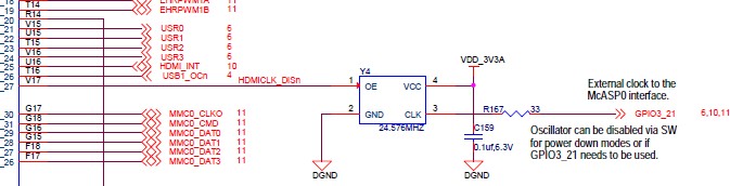
There is an I2S audio interface between the processor and the TDA19988. Stereo audio can be transported over the HDMI interface to an audio equipped display. In order to create the required clock frequencies, and external 24.576MHz oscillator, Y4, is used. From this clock, the processor generates the required clock frequencies for the TDA19988.

There are three signals used to pass data from the processor to the TDA19988. SCLK is the serial clock. SPI1_CS0 is the data pin to the TDA199888. SPI1_D0 is the word sync pin. These signals are configured as I2S interfaces.

Audio is limited to CEA supported resolutions. LCD panels only activate the audio in CEA modes. This is a function of the specification and is not something that can be fixed on the board via a hardware change or a software change.

In order to create the correct clock frequencies, we had to add an external 24.576MHZ oscillator. Unfortunately this had to be input into the processor using the pin previously used for GPIO3_21. In order to keep GPIO3_21 functionality, we provided a way to disable the oscillator if the need was there to use the pin on the expansion header. Figure 45 shows the oscillator circuitry.

image

Figure 45. 24.576MHZ Oscillator

REF: BBONEBLK_SRM BeagleBone Black System Rev C.1

*Reference Manual *

  1. Power Connections

Figure 46 shows the power connections to the TDA19988 device. All voltage rails for the device are at 1.8V. A filter is provided to minimize any noise from the 1.8V rail getting back into the device.

U11

HDMI_1V8

imageimage

imageTDA19988

DGND

Figure 46. HDMI Power Connections

All of the interfaces between the processor and the TDA19988 are 3.3V tolerant allowing for direct connection.

imageimageREF: BBONEBLK_SRM BeagleBone Black System Rev C.1

___________________ *Reference Manual * ___________________ 1. [[_bookmark153]][[bookmark153]]**HDMI Connector Interface** ________________________________________________________________________________________ *Figure 47* shows the design of the interface between the HDMI Framer and the connector. image:media2/media/image102.png[image] _DVI_+5V _ ________________________________________________________________________________________ image:media2/media/image124.png[image,height=16] ___________________________________________________________________________________________________________________________________________________________________________________________________ DGND DGND [[_bookmark154]]**Figure 47. Connector Interface Circuitry** The connector for the HDMI interface is a microHDMI. It should be noted that this connector has a different pinout than the standard or mini HDMI connectors. D6 and D7 are ESD protection devices. ___________________________________________________________________________________________________________________________________________________________________________________________________ [[ref-bboneblk_srm-beaglebone-black-system-rev-c.1-73]] REF: BBONEBLK_SRM BeagleBone Black System Rev C.1 +++++++++++++++++++++++++++++++++++++++++++++++++ ___________________ *Reference Manual * ___________________ [[usb-host]] USB Host ++++++++ _________________________________________________________________________________________________________________________________________________________________ The board is equipped with a single USB host interface accessible from a single USB Type A female connector. *Figure 48* is the design of the USB Host circuitry. _________________________________________________________________________________________________________________________________________________________________ VDD_3V3A _______ SY S_5V _______ R52 _________________________________________ U8 10K,1% USB1_VBUS FB8 image:media2/media/image125.png[image]1 2 0.1Ohm,0805 _________________________________________ FB7 _________________________ P3 USB-A Conn. - 87520-xx1xx 2 8 IN1 OUT1 _________________________ USB1_PWR ________________ 1 2 1 VBUS 5 SHIELD __USB1_DRVVBU__S 3 7 4 IN2 OUT2 6 EN OUT3 USB1_DM USB1_DP 150OHM800mA ________________ 1. D- 2. D+ ________ C34 _+_ 1 5 GND OC 9 PAD ________ 4 GND __________ U9 1 6 6 SHIELD 100uF,6.3V __________ DGND _____________ R53 10K,1% DGND DGND TPS2051 (DGN) DGND D+ VBUS _____________ 2 ___________ D- 5 3 NC ID 4 GND C35 0.1uf ,6.3V DGND USB HOST ___________ TPD4S012 __________________________________________________________________________________________________________________________________________________________________ DGND USB1_OCn 3 image:media2/media/image1.png[image,width=194,height=34]image:media2/media/image2.jpeg[image,width=172,height=27][[_bookmark156]]**Figure 48. USB Host Circuitry** __________________________________________________________________________________________________________________________________________________________________ 1. [[_bookmark157]][[bookmark157]]**Power Switch** __________________________________________________________________________________________________________________________________________________________________________________________________________________________________________________________________________________________________ *U8* is a switch that allows the power to the connector to be turned on or off by the processor. It also has an over current detection that can alert the processor if the current gets too high via the *USB1_OC* signal. The power is controlled by the *USB1_DRVBUS* signal from the processor. __________________________________________________________________________________________________________________________________________________________________________________________________________________________________________________________________________________________________ 1. [[_bookmark158]][[bookmark158]]**ESD Protection** ____________________________________________________________________ *U9* is the ESD protection for the signals that go to the connector. ____________________________________________________________________ 1. [[_bookmark159]][[bookmark159]]**Filter Options** ___________________________________________________________________________________________________________________________________________________________________________________________________________________________________________ *FB7* and *FB8* were added to assist in passing the FCC emissions test. The *USB1_VBUS* signal is used by the processor to detect that the 5V is present on the connector. *FB7* is populated and *FB8* is replaced with a .1 ohm resistor. ___________________________________________________________________________________________________________________________________________________________________________________________________________________________________________ [[ref-bboneblk_srm-beaglebone-black-system-rev-c.1-74]] image:media2/media/image1.png[image,width=194,height=34]image:media2/media/image2.jpeg[image,width=172,height=27]REF: BBONEBLK_SRM BeagleBone Black System Rev C.1
Reference Manual
PRU-ICSS

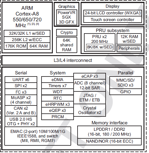
The PRU-ICSS module is located inside the AM3358 processor. Access to these pins is provided by the expansion headers and is multiplexed with other functions on the board. Access is not provided to all of the available pins.

All documentation is located at http://github.com/beagleboard/am335x_pru_package. This feature is not supported by Texas Instruments.

  1. PRU-ICSS Features

The features of the PRU-ICSS include:

Two independent programmable real-time (PRU) cores:

  • 32-Bit Load/Store RISC architecture

  • 8K Byte instruction RAM (2K instructions) per core

  • 8K Bytes data RAM per core

  • 12K Bytes shared RAM

  • Operating frequency of 200 MHz

  • PRU operation is little endian similar to ARM processor

  • All memories within PRU-ICSS support parity

  • Includes Interrupt Controller for system event handling

  • Fast I/O interface

    • 16 input pins and 16 output pins per PRU core. (Not all of these are accessible on the BeagleBone Black).

      1. PRU-ICSS Block Diagram

Figure 49 is a high level block diagram of the PRU-ICSS.

image

Figure 49. PRU-ICSS Block Diagram

imageimageREF: BBONEBLK_SRM BeagleBone Black System Rev C.1

___________________ *Reference Manual * ___________________ 1. [[_bookmark164]][[bookmark164]]**PRU-ICSS Pin Access** ___________________________________________________________________________________________________________________________________________________________________________________________________________________ Both PRU 0 and PRU1 are accessible from the expansion headers. Some may not be useable without first disabling functions on the board like LCD for example. Listed below is what ports can be accessed on each PRU. PRU0 ___________________________________________________________________________________________________________________________________________________________________________________________________________________ * 8 outputs or 9 inputs PRU1 * 13 outputs or 14 inputs * UART0_TXD, UART0_RXD, UART0_CTS, UART0_RTS _____________________________________________________________________________________________________________________________________________________________________________________________ *Table 11* below shows which PRU-ICSS signals can be accessed on the BeagleBone Black and on which connector and pins they are accessible from. Some signals are accessible on the same pins. [[_bookmark165]]**Table 11. PRU0 and PRU1 Access** _____________________________________________________________________________________________________________________________________________________________________________________________ [cols=",,,,,,",options="header",] |============================================ | a| _____ *PIN* _____ a| ______ *PROC* ______ a| ______ *NAME* ______ | | | a| __ P8 __ a| __ 11 __ a| ___ R12 ___ |GPIO1_13 | a| ______________________________ *pr1_pru0_pru_r30_15 (Output)* ______________________________ | | a| __ 12 __ a| ___ T12 ___ |GPIO1_12 | a| ______________________________ *pr1_pru0_pru_r30_14 (Output)* ______________________________ | | a| __ 15 __ a| ___ U13 ___ |GPIO1_15 | a| _____________________________ *pr1_pru0_pru_r31_15 (Input)* _____________________________ | | a| __ 16 __ a| ___ V13 ___ |GPIO1_14 | a| _____________________________ *pr1_pru0_pru_r31_14 (Input)* _____________________________ | | a| __ 20 __ a| __ V9 __ |GPIO1_31 |pr1_pru1_pru_r30_13 (Output) a| ___________________________ pr1_pru1_pru_r31_13 (INPUT) ___________________________ | | a| __ 21 __ a| __ U9 __ |GPIO1_30 |pr1_pru1_pru_r30_12 (Output) a| ___________________________ pr1_pru1_pru_r31_12 (INPUT) ___________________________ | | a| __ 27 __ a| __ U5 __ |GPIO2_22 |pr1_pru1_pru_r30_8 (Output) a| __________________________ pr1_pru1_pru_r31_8 (INPUT) __________________________ | | a| __ 28 __ a| __ V5 __ |GPIO2_24 |pr1_pru1_pru_r30_10 (Output) a| ___________________________ pr1_pru1_pru_r31_10 (INPUT) ___________________________ | | a| __ 29 __ a| __ R5 __ |GPIO2_23 |pr1_pru1_pru_r30_9 (Output) a| __________________________ pr1_pru1_pru_r31_9 (INPUT) __________________________ | | a| __ 39 __ a| __ T3 __ |GPIO2_12 |pr1_pru1_pru_r30_6 (Output) a| __________________________ pr1_pru1_pru_r31_6 (INPUT) __________________________ | | a| __ 40 __ a| __ T4 __ |GPIO2_13 |pr1_pru1_pru_r30_7 (Output) a| __________________________ pr1_pru1_pru_r31_7 (INPUT) __________________________ | | a| __ 41 __ a| __ T1 __ |GPIO2_10 |pr1_pru1_pru_r30_4 (Output) a| __________________________ pr1_pru1_pru_r31_4 (INPUT) __________________________ | | a| __ 42 __ a| __ T2 __ |GPIO2_11 |pr1_pru1_pru_r30_5 (Output) a| __________________________ pr1_pru1_pru_r31_5 (INPUT) __________________________ | | a| __ 43 __ a| __ R3 __ |GPIO2_8 |pr1_pru1_pru_r30_2 (Output) a| __________________________ pr1_pru1_pru_r31_2 (INPUT) __________________________ | | a| __ 44 __ a| __ R4 __ |GPIO2_9 |pr1_pru1_pru_r30_3 (Output) a| __________________________ pr1_pru1_pru_r31_3 (INPUT) __________________________ | | a| __ 45 __ a| __ R1 __ |GPIO2_6 |pr1_pru1_pru_r30_0 (Output) a| __________________________ pr1_pru1_pru_r31_0 (INPUT) __________________________ | | a| __ 46 __ a| __ R2 __ |GPIO2_7 |pr1_pru1_pru_r30_1 (Output) a| __________________________ pr1_pru1_pru_r31_1 (INPUT) __________________________ | | | | | | | | a| __ P9 __ a| __ 17 __ a| ___ A16 ___ |I2C1_SCL a| _____________ pr1_uart0_txd _____________ | | | a| __ 18 __ a| ___ B16 ___ |I2C1_SDA a| _____________ pr1_uart0_rxd _____________ | | | a| __ 19 __ a| ___ D17 ___ |I2C2_SCL a| _______________ pr1_uart0_rts_n _______________ | | | a| __ 20 __ a| ___ D18 ___ |I2C2_SDA a| _______________ pr1_uart0_cts_n _______________ | | | a| __ 21 __ a| ___ B17 ___ |UART2_TXD a| _______________ pr1_uart0_rts_n _______________ | | | a| __ 22 __ a| ___ A17 ___ |UART2_RXD a| _______________ pr1_uart0_cts_n _______________ | | | a| __ 24 __ a| ___ D15 ___ |UART1_TXD a| _____________ pr1_uart0_txd _____________ a| _____________________________ *pr1_pru0_pru_r31_16 (Input)* _____________________________ | | a| __ 25 __ a| ___ A14 ___ |GPIO3_21* |*pr1_pru0_pru_r30_5 (Output)* a| ____________________________ *pr1_pru0_pru_r31_5((Input)* ____________________________ | | a| __ 26 __ a| ___ D16 ___ |UART1_RXD a| _____________ pr1_uart0_rxd _____________ a| ___________________ pr1_pru1_pru_r31_16 ___________________ | | a| __ 27 __ a| ___ C13 ___ |GPIO3_19 |*pr1_pru0_pru_r30_7 (Output)* a| ____________________________ *pr1_pru0_pru_r31_7 (Input)* ____________________________ | | a| __ 28 __ a| ___ C12 ___ |SPI1_CS0 a| _________________ eCAP2_in_PWM2_out _________________ a| _____________________________ *pr1_pru0_pru_r30_3 (Output)* _____________________________ a| ____________________________ *pr1_pru0_pru_r31_3 (Input)* ____________________________ | a| __ 29 __ a| ___ B13 ___ a| _______ SPI1_D0 _______ |*pr1_pru0_pru_r30_1 (Output)* a| ____________________________ *pr1_pru0_pru_r31_1 (Input)* ____________________________ | | a| __ 30 __ a| ___ D12 ___ a| _______ SPI1_D1 _______ |*pr1_pru0_pru_r30_2 (Output)* a| ____________________________ *pr1_pru0_pru_r31_2 (Input)* ____________________________ | | a| __ 31 __ a| ___ A13 ___ |SPI1_SCLK |*pr1_pru0_pru_r30_0 (Output)* a| ____________________________ *pr1_pru0_pru_r31_0 (Input)* ____________________________ | |============================================ [[ref-bboneblk_srm-beaglebone-black-system-rev-c.1-76]] image:media2/media/image1.png[image,width=194,height=34]image:media2/media/image2.jpeg[image,width=172,height=27]REF: BBONEBLK_SRM BeagleBone Black System Rev C.1

*Reference Manual *

Connectors

This section describes each of the connectors on the board.

Expansion Connectors

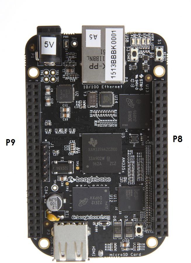
The expansion interface on the board is comprised of two 46 pin connectors. All signals on the expansion headers are 3.3V unless otherwise indicated.

NOTE: Do not connect 5V logic level signals to these pins or the board will be damaged.

NOTE: DO NOT APPLY VOLTAGE TO ANY I/O PIN WHEN POWER IS NOT SUPPLIED TO THE BOARD. IT WILL DAMAGE THE PROCESSOR AND VOID THE WARRANTY.

NO PINS ARE TO BE DRIVEN UNTIL AFTER THE SYS_RESET LINE GOES HIGH.

Figure 50 shows the location of the expansion connectors.

image

Figure 50. Expansion Connector Location

The location and spacing of the expansion headers are the same as on the original BeagleBone.

imageimageREF: BBONEBLK_SRM BeagleBone Black System Rev C.1

___________________ *Reference Manual * ___________________ 1. [[_bookmark169]][[bookmark169]]**Connector P8** _________________________________________________________________________________________________________________________________________________________________________________________________________________________________________________________________________________________________________________________________________________________________________________________________________________________________________________________________________________________________________________________________________________________________________________________________ *Table 12* shows the pinout of the *P8* expansion header. Other signals can be connected to this connector based on setting the pin mux on the processor, but this is the default settings on power up. The SW is responsible for setting the default function of each pin. There are some signals that have not been listed here. Refer to the processor documentation for more information on these pins and detailed descriptions of all of the pins listed. In some cases there may not be enough signals to complete a group of signals that may be required to implement a total interface. The *PROC* column is the pin number on the processor. The *PIN* column is the pin number on the expansion header. The *MODE* columns are the mode setting for each pin. Setting each mode to align with the mode column will give that function on that pin. *NOTE: DO NOT APPLY VOLTAGE TO ANY I/O PIN WHEN POWER IS NOT SUPPLIED TO THE BOARD. IT WILL DAMAGE THE PROCESSOR AND VOID THE WARRANTY.* *NO PINS ARE TO BE DRIVEN UNTIL AFTER THE SYS_RESET LINE GOES HIGH.* image:media2/media/image1.png[image,width=194,height=34]image:media2/media/image2.jpeg[image,width=172,height=27]*REF: BBONEBLK_SRM BeagleBone Black System Rev C.1* *Reference Manual * _________________________________________________________________________________________________________________________________________________________________________________________________________________________________________________________________________________________________________________________________________________________________________________________________________________________________________________________________________________________________________________________________________________________________________________________________ [[_bookmark170]]**Table 12. Expansion Header P8 Pinout** [cols=",",options="header",] |================== a| _____ *PIN* _____ |*PROC* a| ______ *NAME* ______ a| _______ *MODE0* _______ a| _______ *MODE1* _______ a| _______ *MODE2* _______ a| _______ *MODE3* _______ a| _______ *MODE4* _______ a| _______ *MODE5* _______ a| _______ *MODE6* _______ a| _______ *MODE7* _______ a| ___ 1,2 ___ a| _____ *GND* _____ |3 |R9 a| _______ GPIO1_6 _______ a| ________ gpmc_ad6 ________ a| _________ mmc1_dat6 _________ | | | | | a| ________ gpio1[6] ________ |4 |T9 a| _______ GPIO1_7 _______ a| ________ gpmc_ad7 ________ a| _________ mmc1_dat7 _________ | | | | | a| ________ gpio1[7] ________ |5 |R8 a| _______ GPIO1_2 _______ a| ________ gpmc_ad2 ________ a| _________ mmc1_dat2 _________ | | | | | a| ________ gpio1[2] ________ |6 |T8 a| _______ GPIO1_3 _______ a| ________ gpmc_ad3 ________ a| _________ mmc1_dat3 _________ | | | | | a| ________ gpio1[3] ________ |7 |R7 a| ______ TIMER4 ______ a| _____________ gpmc_advn_ale _____________ | a| ______ timer4 ______ | | | | a| ________ gpio2[2] ________ |8 |T7 a| ______ TIMER7 ______ a| ____________ gpmc_oen_ren ____________ | a| ______ timer7 ______ | | | | a| ________ gpio2[3] ________ |9 |T6 a| ______ TIMER5 ______ a| _____________ gpmc_be0n_cle _____________ | a| ______ timer5 ______ | | | | a| ________ gpio2[5] ________ a| __ 10 __ |U6 a| ______ TIMER6 ______ a| ________ gpmc_wen ________ | a| ______ timer6 ______ | | | | a| ________ gpio2[4] ________ a| __ 11 __ |R12 a| ________ GPIO1_13 ________ a| _________ gpmc_ad13 _________ a| __________ lcd_data18 __________ a| _________ mmc1_dat5 _________ a| _________ mmc2_dat1 _________ a| _________ eQEP2B_in _________ | a| ___________________ pr1_pru0_pru_r30_15 ___________________ a| _________ gpio1[13] _________ a| __ 12 __ |T12 a| ________ GPIO1_12 ________ a| _________ gpmc_ad12 _________ a| __________ Lcd_data19 __________ a| _________ mmc1_dat4 _________ a| _________ Mmc2_dat0 _________ a| _________ Eqep2a_in _________ | a| ___________________ pr1_pru0_pru_r30_14 ___________________ a| _________ gpio1[12] _________ a| __ 13 __ |T10 a| ________ EHRPWM2B ________ a| ________ gpmc_ad9 ________ a| __________ lcd_data22 __________ a| _________ mmc1_dat1 _________ a| _________ mmc2_dat5 _________ a| ________ ehrpwm2B ________ | | a| _________ gpio0[23] _________ a| __ 14 __ |T11 a| ________ GPIO0_26 ________ a| _________ gpmc_ad10 _________ a| __________ lcd_data21 __________ a| _________ mmc1_dat2 _________ a| _________ mmc2_dat6 _________ a| ___________________ ehrpwm2_tripzone_in ___________________ | | a| _________ gpio0[26] _________ a| __ 15 __ |U13 a| ________ GPIO1_15 ________ a| _________ gpmc_ad15 _________ a| __________ lcd_data16 __________ a| _________ mmc1_dat7 _________ a| _________ mmc2_dat3 _________ a| ____________ eQEP2_strobe ____________ | a| ___________________ pr1_pru0_pru_r31_15 ___________________ a| _________ gpio1[15] _________ a| __ 16 __ |V13 a| ________ GPIO1_14 ________ a| _________ gpmc_ad14 _________ a| __________ lcd_data17 __________ a| _________ mmc1_dat6 _________ a| _________ mmc2_dat2 _________ a| ___________ eQEP2_index ___________ | a| ___________________ pr1_pru0_pru_r31_14 ___________________ a| _________ gpio1[14] _________ a| __ 17 __ |U12 a| ________ GPIO0_27 ________ a| _________ gpmc_ad11 _________ a| __________ lcd_data20 __________ a| _________ mmc1_dat3 _________ a| _________ mmc2_dat7 _________ a| _____________ ehrpwm0_synco _____________ | | a| _________ gpio0[27] _________ a| __ 18 __ |V12 a| _______ GPIO2_1 _______ a| _____________ gpmc_clk_mux0 _____________ a| ______________ lcd_memory_clk ______________ a| __________ gpmc_wait1 __________ a| ________ mmc2_clk ________ | | a| __________ mcasp0_fsr __________ a| ________ gpio2[1] ________ a| __ 19 __ |U10 a| ________ EHRPWM2A ________ a| ________ gpmc_ad8 ________ a| __________ lcd_data23 __________ a| _________ mmc1_dat0 _________ a| _________ mmc2_dat4 _________ a| ________ ehrpwm2A ________ | | a| _________ gpio0[22] _________ a| __ 20 __ |V9 a| ________ GPIO1_31 ________ a| _________ gpmc_csn2 _________ a| _________ gpmc_be1n _________ a| ________ mmc1_cmd ________ | | a| ___________________ pr1_pru1_pru_r30_13 ___________________ a| ___________________ pr1_pru1_pru_r31_13 ___________________ a| _________ gpio1[31] _________ a| __ 21 __ |U9 a| ________ GPIO1_30 ________ a| _________ gpmc_csn1 _________ a| ________ gpmc_clk ________ a| ________ mmc1_clk ________ | | a| ___________________ pr1_pru1_pru_r30_12 ___________________ a| ___________________ pr1_pru1_pru_r31_12 ___________________ a| _________ gpio1[30] _________ a| __ 22 __ |V8 a| _______ GPIO1_5 _______ a| ________ gpmc_ad5 ________ a| _________ mmc1_dat5 _________ | | | | | a| ________ gpio1[5] ________ a| __ 23 __ |U8 a| _______ GPIO1_4 _______ a| ________ gpmc_ad4 ________ a| _________ mmc1_dat4 _________ | | | | | a| ________ gpio1[4] ________ a| __ 24 __ |V7 a| _______ GPIO1_1 _______ a| ________ gpmc_ad1 ________ a| _________ mmc1_dat1 _________ | | | | | a| ________ gpio1[1] ________ a| __ 25 __ |U7 a| _______ GPIO1_0 _______ a| ________ gpmc_ad0 ________ a| _________ mmc1_dat0 _________ | | | | | a| ________ gpio1[0] ________ a| __ 26 __ |V6 a| ________ GPIO1_29 ________ a| _________ gpmc_csn0 _________ | | | | | | a| _________ gpio1[29] _________ a| __ 27 __ |U5 a| ________ GPIO2_22 ________ a| _________ lcd_vsync _________ a| _______ gpmc_a8 _______ | | | a| __________________ pr1_pru1_pru_r30_8 __________________ a| __________________ pr1_pru1_pru_r31_8 __________________ a| _________ gpio2[22] _________ a| __ 28 __ |V5 a| ________ GPIO2_24 ________ a| ________ lcd_pclk ________ a| ________ gpmc_a10 ________ | | | a| ___________________ pr1_pru1_pru_r30_10 ___________________ a| ___________________ pr1_pru1_pru_r31_10 ___________________ a| _________ gpio2[24] _________ a| __ 29 __ |R5 a| ________ GPIO2_23 ________ a| _________ lcd_hsync _________ a| _______ gpmc_a9 _______ | | | a| __________________ pr1_pru1_pru_r30_9 __________________ a| __________________ pr1_pru1_pru_r31_9 __________________ a| _________ gpio2[23] _________ a| __ 30 __ |R6 a| ________ GPIO2_25 ________ a| ______________ lcd_ac_bias_en ______________ a| ________ gpmc_a11 ________ | | | | | a| _________ gpio2[25] _________ a| __ 31 __ |V4 a| __________ UART5_CTSN __________ a| __________ lcd_data14 __________ a| ________ gpmc_a18 ________ a| ___________ eQEP1_index ___________ a| ___________ mcasp0_axr1 ___________ a| _________ uart5_rxd _________ | a| __________ uart5_ctsn __________ a| _________ gpio0[10] _________ a| __ 32 __ |T5 a| __________ UART5_RTSN __________ a| __________ lcd_data15 __________ a| ________ gpmc_a19 ________ a| ____________ eQEP1_strobe ____________ a| _____________ mcasp0_ahclkx _____________ a| ___________ mcasp0_axr3 ___________ | a| __________ uart5_rtsn __________ a| _________ gpio0[11] _________ a| __ 33 __ |V3 a| __________ UART4_RTSN __________ a| __________ lcd_data13 __________ a| ________ gpmc_a17 ________ a| _________ eQEP1B_in _________ a| __________ mcasp0_fsr __________ a| ___________ mcasp0_axr3 ___________ | a| __________ uart4_rtsn __________ a| ________ gpio0[9] ________ a| __ 34 __ |U4 a| __________ UART3_RTSN __________ a| __________ lcd_data11 __________ a| ________ gpmc_a15 ________ a| ________ ehrpwm1B ________ a| _____________ mcasp0_ahclkr _____________ a| ___________ mcasp0_axr2 ___________ | a| __________ uart3_rtsn __________ a| _________ gpio2[17] _________ a| __ 35 __ |V2 a| __________ UART4_CTSN __________ a| __________ lcd_data12 __________ a| ________ gpmc_a16 ________ a| _________ eQEP1A_in _________ a| ____________ mcasp0_aclkr ____________ a| ___________ mcasp0_axr2 ___________ | a| __________ uart4_ctsn __________ a| ________ gpio0[8] ________ a| __ 36 __ |U3 a| __________ UART3_CTSN __________ a| __________ lcd_data10 __________ a| ________ gpmc_a14 ________ a| ________ ehrpwm1A ________ a| ___________ mcasp0_axr0 ___________ | | a| __________ uart3_ctsn __________ a| _________ gpio2[16] _________ a| __ 37 __ |U1 a| _________ UART5_TXD _________ a| _________ lcd_data8 _________ a| ________ gpmc_a12 ________ a| ___________________ ehrpwm1_tripzone_in ___________________ a| ____________ mcasp0_aclkx ____________ a| _________ uart5_txd _________ | a| __________ uart2_ctsn __________ a| _________ gpio2[14] _________ a| __ 38 __ |U2 a| _________ UART5_RXD _________ a| _________ lcd_data9 _________ a| ________ gpmc_a13 ________ a| _____________ ehrpwm0_synco _____________ a| __________ mcasp0_fsx __________ a| _________ uart5_rxd _________ | a| __________ uart2_rtsn __________ a| _________ gpio2[15] _________ a| __ 39 __ |T3 a| ________ GPIO2_12 ________ a| _________ lcd_data6 _________ a| _______ gpmc_a6 _______ | a| ___________ eQEP2_index ___________ | a| __________________ pr1_pru1_pru_r30_6 __________________ a| __________________ pr1_pru1_pru_r31_6 __________________ a| _________ gpio2[12] _________ a| __ 40 __ |T4 a| ________ GPIO2_13 ________ a| _________ lcd_data7 _________ a| _______ gpmc_a7 _______ | a| ____________ eQEP2_strobe ____________ a| __________________ pr1_edio_data_out7 __________________ a| __________________ pr1_pru1_pru_r30_7 __________________ a| __________________ pr1_pru1_pru_r31_7 __________________ a| _________ gpio2[13] _________ a| __ 41 __ |T1 a| ________ GPIO2_10 ________ a| _________ lcd_data4 _________ a| _______ gpmc_a4 _______ | a| _________ eQEP2A_in _________ | a| __________________ pr1_pru1_pru_r30_4 __________________ a| __________________ pr1_pru1_pru_r31_4 __________________ a| _________ gpio2[10] _________ a| __ 42 __ |T2 a| ________ GPIO2_11 ________ a| _________ lcd_data5 _________ a| _______ gpmc_a5 _______ | a| _________ eQEP2B_in _________ | a| __________________ pr1_pru1_pru_r30_5 __________________ a| __________________ pr1_pru1_pru_r31_5 __________________ a| _________ gpio2[11] _________ a| __ 43 __ |R3 a| _______ GPIO2_8 _______ a| _________ lcd_data2 _________ a| _______ gpmc_a2 _______ | a| ___________________ ehrpwm2_tripzone_in ___________________ | a| __________________ pr1_pru1_pru_r30_2 __________________ a| __________________ pr1_pru1_pru_r31_2 __________________ a| ________ gpio2[8] ________ a| __ 44 __ |R4 a| _______ GPIO2_9 _______ a| _________ lcd_data3 _________ a| _______ gpmc_a3 _______ | a| _____________ ehrpwm0_synco _____________ | a| __________________ pr1_pru1_pru_r30_3 __________________ a| __________________ pr1_pru1_pru_r31_3 __________________ a| ________ gpio2[9] ________ a| __ 45 __ |R1 a| _______ GPIO2_6 _______ a| _________ lcd_data0 _________ a| _______ gpmc_a0 _______ | a| ________ ehrpwm2A ________ | a| __________________ pr1_pru1_pru_r30_0 __________________ a| __________________ pr1_pru1_pru_r31_0 __________________ a| ________ gpio2[6] ________ a| __ 46 __ |R2 a| _______ GPIO2_7 _______ a| _________ lcd_data1 _________ a| _______ gpmc_a1 _______ | a| ________ ehrpwm2B ________ | a| __________________ pr1_pru1_pru_r30_1 __________________ a| __________________ pr1_pru1_pru_r31_1 __________________ a| ________ gpio2[7] ________ |================== [[ref-bboneblk_srm-beaglebone-black-system-rev-c.1-78]] image:media2/media/image1.png[image,width=194,height=34]image:media2/media/image2.jpeg[image,width=172,height=27]REF: BBONEBLK_SRM BeagleBone Black System Rev C.1

*Reference Manual *

  1. Connector P9

Table 13 lists the signals on connector P9. Other signals can be connected to this connector based on setting the pin mux on the processor, but this is the default settings on power up.

There are some signals that have not been listed here. Refer to the processor documentation for more information on these pins and detailed descriptions of all of the pins listed. In some cases there may not be enough signals to complete a group of signals that may be required to implement a total interface.

The PROC column is the pin number on the processor.

The PIN column is the pin number on the expansion header.

The MODE columns are the mode setting for each pin. Setting each mode to align with the mode column will give that function on that pin.

NOTES:

In the table are the following notations:

PWR_BUT is a 5V level as pulled up internally by the TPS65217C. It is activated by pulling the signal to GND.

# Both of these signals connect to pin 41 of P11. Resistors are installed that allow for the GPIO3_20 connection to be removed by removing R221. The intent is to allow the SW to use either of these signals, one or the other, on pin 41. SW should set the unused pin in input mode when using the other pin. This allowed us to get an extra signal out to the expansion header.

@ Both of these signals connect to pin 42 of P11. Resistors are installed that allow for the GPIO3_18 connection to be removed by removing R202. The intent is to allow the SW to use either of these signals, on pin 42. SW should set the unused pin in input mode when using the other pin. This allowed us to get an extra signal out to the expansion header.

NOTE: DO NOT APPLY VOLTAGE TO ANY I/O PIN WHEN POWER IS NOT SUPPLIED TO THE BOARD. IT WILL DAMAGE THE PROCESSOR AND VOID THE WARRANTY.

NO PINS ARE TO BE DRIVEN UNTIL AFTER THE SYS_RESET LINE GOES HIGH.

imageimageREF: BBONEBLK_SRM BeagleBone Black System Rev C.1

*Reference Manual *

Table 13. Expansion Header P9 Pinout

PIN PROC

NAME

MODE0

MODE1

MODE2

MODE3

MODE4

MODE5

MODE6

MODE7


1,2 _


GND _


3,4 _

DC_3.3V


5,6 _

VDD_5V


7,8 _

SYS_5V

9

PWR_BUT

10


A10 _

SYS_RESETn

11


T17 _

UART4_RXD

gpmc_wait0

mii2_crs

gpmc_csn4

rmii2_crs_dv

mmc1_sdcd

uart4_rxd_mux2

gpio0[30]

12


U18 _

GPIO1_28

gpmc_be1n

mii2_col

gpmc_csn6

mmc2_dat3

gpmc_dir

mcasp0_aclkr_mux3

gpio1[28]

13


U17 _

UART4_TXD

gpmc_wpn

mii2_rxerr

gpmc_csn5

rmii2_rxerr

mmc2_sdcd

uart4_txd_mux2

gpio0[31]

14


U14 _

EHRPWM1A

gpmc_a2

mii2_txd3

rgmii2_td3

mmc2_dat1

gpmc_a18

ehrpwm1A_mux1

gpio1[18]

15


R13 _

GPIO1_16

gpmc_a0

gmii2_txen

rmii2_tctl

mii2_txen

gpmc_a16

ehrpwm1_tripzone_input

gpio1[16]

16


T14 _

EHRPWM1B

gpmc_a3

mii2_txd2

rgmii2_td2

mmc2_dat2

gpmc_a19

ehrpwm1B_mux1

gpio1[19]

17


A16 _

I2C1_SCL

spi0_cs0

mmc2_sdwp

I2C1_SCL

ehrpwm0_synci

pr1_uart0_txd

gpio0[5]

18


B16 _

I2C1_SDA

spi0_d1

mmc1_sdwp

I2C1_SDA

ehrpwm0_tripzone

pr1_uart0_rxd

gpio0[4]

19


D17 _

I2C2_SCL

uart1_rtsn

timer5

dcan0_rx

I2C2_SCL

spi1_cs1

pr1_uart0_rts_n

gpio0[13]

20


D18 _

I2C2_SDA

uart1_ctsn

timer6

dcan0_tx

I2C2_SDA

spi1_cs0

pr1_uart0_cts_n

gpio0[12]

21


B17 _

UART2_TXD

spi0_d0

uart2_txd

I2C2_SCL

ehrpwm0B

pr1_uart0_rts_n

EMU3_mux1

gpio0[3]

22


A17 _

UART2_RXD

spi0_sclk

uart2_rxd

I2C2_SDA

ehrpwm0A

pr1_uart0_cts_n

EMU2_mux1

gpio0[2]

23


V14 _

GPIO1_17

gpmc_a1

gmii2_rxdv

rgmii2_rxdv

mmc2_dat0

gpmc_a17

ehrpwm0_synco

gpio1[17]

24


D15 _

UART1_TXD

uart1_txd

mmc2_sdwp

dcan1_rx

I2C1_SCL

pr1_uart0_txd

pr1_pru0_pru_r31_16

gpio0[15]

25


A14 _

GPIO3_21*

mcasp0_ahclkx

eQEP0_strobe

mcasp0_axr3

mcasp1_axr1

EMU4_mux2

pr1_pru0_pru_r30_7

pr1_pru0_pru_r31_7

gpio3[21]

26


D16 _

UART1_RXD

uart1_rxd

mmc1_sdwp

dcan1_tx

I2C1_SDA

pr1_uart0_rxd

pr1_pru1_pru_r31_16

gpio0[14]

27


C13 _

GPIO3_19

mcasp0_fsr

eQEP0B_in

mcasp0_axr3

mcasp1_fsx

EMU2_mux2

pr1_pru0_pru_r30_5

pr1_pru0_pru_r31_5

gpio3[19]

28


C12 _

SPI1_CS0

mcasp0_ahclkr

ehrpwm0_synci

mcasp0_axr2

spi1_cs0

eCAP2_in_PWM2_out

pr1_pru0_pru_r30_3

pr1_pru0_pru_r31_3

gpio3[17]

29


B13 _

SPI1_D0

mcasp0_fsx

ehrpwm0B

spi1_d0

mmc1_sdcd_mux1

pr1_pru0_pru_r30_1

pr1_pru0_pru_r31_1

gpio3[15]

30


D12 _

SPI1_D1

mcasp0_axr0

ehrpwm0_tripzone

spi1_d1

mmc2_sdcd_mux1

pr1_pru0_pru_r30_2

pr1_pru0_pru_r31_2

gpio3[16]

31


A13 _

SPI1_SCLK

mcasp0_aclkx

ehrpwm0A

spi1_sclk

mmc0_sdcd_mux1

pr1_pru0_pru_r30_0

pr1_pru0_pru_r31_0

gpio3[14]

32

VADC

33

C8

AIN4

34

AGND

35

A8

AIN6

36

B8

AIN5

37

B7

AIN2

38

A7

AIN3

39

B6

AIN0

40

C7

AIN1


41# _


D14 _

CLKOUT2

xdma_event_intr1

tclkin

clkout2

timer7_mux1

pr1_pru0_pru_r31_16

EMU3_mux0

gpio0[20]


D13 _

GPIO3_20

mcasp0_axr1

eQEP0_index

Mcasp1_axr0

emu3

pr1_pru0_pru_r30_6

pr1_pru0_pru_r31_6

gpio3[20]


42@ _


C18 _

GPIO0_7

eCAP0_in_PWM0_out

uart3_txd

spi1_cs1

pr1_ecap0_ecap_capin_apwm_o

spi1_sclk

mmc0_sdwp

xdma_event_intr2

gpio0[7]


B12 _

GPIO3_18

Mcasp0_aclkr

eQEP0A_in

Mcaspo_axr2

Mcasp1_aclkx

pr1_pru0_pru_r30_4

pr1_pru0_pru_r31_4

gpio3[18]

43-46


GND _

** GPIO3_21 is also the 24.576MHZ clock input to the processor to enable HDMI audio. To use this pin the oscillator must be disabled.*

imageimageREF: BBONEBLK_SRM BeagleBone Black System Rev C.1

___________________ *Reference Manual * ___________________ [[power-jack]] Power Jack ++++++++++ _______________________________________________________________________________________________________________________________________________________________________________________________ The DC power jack is located next to the RJ45 Ethernet connector as shown in *Figure* *51*. This uses the same power connector as is used on the original BeagleBone. The connector has a 2.1mm diameter center post (5VDC) and a 5.5mm diameter outer dimension on the barrel (GND). _______________________________________________________________________________________________________________________________________________________________________________________________ image:media2/media/image134.jpeg[image] _______________________________________________________________________________________________________________________________________________________________________________________________________________ [[_bookmark174]]**Figure 51. 5VDC Power Jack** The board requires a regulated 5VDC +/-.25V supply at 1A. A higher current rating may be needed if capes are plugged into the expansion headers. Using a higher current power supply will not damage the board. _______________________________________________________________________________________________________________________________________________________________________________________________________________ [[ref-bboneblk_srm-beaglebone-black-system-rev-c.1-80]] image:media2/media/image1.png[image,width=194,height=34]image:media2/media/image2.jpeg[image,width=172,height=27]REF: BBONEBLK_SRM BeagleBone Black System Rev C.1

*Reference Manual *

USB Client

The USB Client connector is accessible on the bottom side of the board under the row of four LEDs as shown in Figure 52. It uses a 5 pin miniUSB cable, the same as is used on the original BeagleBone. The cable is provided with the board. The cable can also be used to power the board.

image

Figure 52. USB Client Connector

This port is a USB Client only interface and is intended for connection to a PC.

imageimageREF: BBONEBLK_SRM BeagleBone Black System Rev C.1

___________________ *Reference Manual * ___________________ [[usb-host-1]] USB Host ++++++++ ____________________________________________________________________________________ There is a single USB Host connector on the board and is shown in *Figure 53* below. ____________________________________________________________________________________ image:media2/media/image135.jpeg[image] ____________________________________________________________________________________________________________________________________ [[_bookmark178]]**Figure 53. USB Host Connector** The port is USB 2.0 HS compatible and can supply up to 500mA of current. If more current or ports is needed, then a HUB can be used. ____________________________________________________________________________________________________________________________________ [[ref-bboneblk_srm-beaglebone-black-system-rev-c.1-82]] image:media2/media/image1.png[image,width=194,height=34]image:media2/media/image2.jpeg[image,width=172,height=27]REF: BBONEBLK_SRM BeagleBone Black System Rev C.1

*Reference Manual *

Serial Header

Each board has a debug serial interface that can be accessed by using a special serial cable that is plugged into the serial header as shown in Figure 54 below.

image

Figure 54. Serial Debug Header

Two signals are provided, TX and RX on this connector. The levels on these signals are 3.3V. In order to access these signals, a FTDI USB to Serial cable is recommended as shown in Figure 55 below.

imageSerial Debug Cable Pin 1

Figure 55. FTDI USB to Serial Adapter

The cable can be purchased from several different places and must be the 3.3V version TTL-232R-3V3. Information on the cable itself can be found direct from FTDI at: http://www.ftdichip.com/Support/Documents/DataSheets/Cables/DS_TTL- 232R_CABLES.pdf

imageimageREF: BBONEBLK_SRM BeagleBone Black System Rev C.1

_______________________________________________________________________________________________________________________________________________________________________________________________________________________________________________________________________________________________________________________________________________________________________________________________________________________________________________________________________________________________________________________________________________________ *Reference Manual * Pin 1 of the cable is the black wire. That must align with the pin 1 on the board which is designated by the white dot next to the connector on the board. Refer to the support WIKI http://circuitco.com/support/index.php?title=BeagleBoneBlack[_http://circuitco.com/support/index.php?title=BeagleBoneBlack_] for more sources of this cable and other options that will work. Table is the pinout of the connector as reflected in the schematic. It is the same as the FTDI cable which can be found at http://www.ftdichip.com/Support/Documents/DataSheets/Cables/DS_TTL-232R_CABLES.pdf[_http://www.ftdichip.com/Support/Documents/DataSheets/Cables/DS_TTL-_] http://www.ftdichip.com/Support/Documents/DataSheets/Cables/DS_TTL-232R_CABLES.pdf[_232R_CABLES.pdf_] with the exception that only three pins are used on the board. The pin numbers are defined in *Table 14*. The signals are from the perspective of the board. [[_bookmark182]]**Table 14. J1 Serial Header Pins** _______________________________________________________________________________________________________________________________________________________________________________________________________________________________________________________________________________________________________________________________________________________________________________________________________________________________________________________________________________________________________________________________________________________ [cols="",options="header",] |======= a| ______ Ground ______ a| _______ Receive _______ a| ________ Transmit ________ |======= ________________________________________________ *Figure 56* shows the pin location on the board. image:media2/media/image137.jpeg[image]PIN 1 PIN4 PIN 5 [[_bookmark183]]**Figure 56. Serial Header** ________________________________________________ [[ref-bboneblk_srm-beaglebone-black-system-rev-c.1-84]] image:media2/media/image1.png[image,width=194,height=34]image:media2/media/image2.jpeg[image,width=172,height=27]REF: BBONEBLK_SRM BeagleBone Black System Rev C.1

*Reference Manual *

HDMI

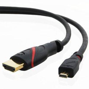
Access to the HDMI interface is through the HDMI connector that is located on the bottom side of the board as shown in Figure 57 below.

image

Figure 57. HDMI Connector

The connector is microHDMI connector. This was done due to the space limitations we had in finding a place to fit the connector. It requires a microHDMI to HDMI cable as shown in Figure 58 below. The cable can be purchased from several different sources.

Mediabridge Micro-HDMI to HDMI Cable with Ethernet - 6 Feet - FLEX Series High Speed

Figure 58. HDMI Cable

imageimageREF: BBONEBLK_SRM BeagleBone Black System Rev C.1

___________________ *Reference Manual * ___________________ [[microsd]] microSD +++++++ ___________________________________________________________________________________________________________________________________________________________________________________________________________________________________________________________________________________________________________________________________________________________________________ A microSD connector is located on the back or bottom side of the board as shown in *Figure 59* below. The microSD card is not supplied with the board. image:media2/media/image135.jpeg[image]microSD Connector [[_bookmark188]]**Figure 59. microSD Connector** When plugging in the SD card, the writing on the card should be up. Align the card with the connector and push to insert. Then release. There should be a click and the card will start to eject slightly, but it then should latch into the connector. To eject the card, push the SD card in and then remove your finger. The SD card will be ejected from the connector. Do not pull the SD card out or you could damage the connector. ___________________________________________________________________________________________________________________________________________________________________________________________________________________________________________________________________________________________________________________________________________________________________________ [[ref-bboneblk_srm-beaglebone-black-system-rev-c.1-86]] image:media2/media/image1.png[image,width=194,height=34]image:media2/media/image2.jpeg[image,width=172,height=27]REF: BBONEBLK_SRM BeagleBone Black System Rev C.1

*Reference Manual *

Ethernet

imageThe board comes with a single 10/100 Ethernet interface located next to the power jack as shown in Figure 60.

Figure 60. Ethernet Connector

The PHY supports AutoMDX which means either a straight or a swap cable can be used

JTAG Connector

A place for an optional 20 pin CTI JTAG header is provided on the board to facilitate the SW development and debugging of the board by using various JTAG emulators. This header is not supplied standard on the board. To use this, a connector will need to be soldered onto the board.

If you need the JTAG connector you can solder it on yourself. No other components are needed. The connector is made by Samtec and the part number is FTR-110-03-G-D-06. You can purchase it from www.digikey.com.

imageimageREF: BBONEBLK_SRM BeagleBone Black System Rev C.1

___________________ *Reference Manual * ___________________ [[cape-board-support-1]] Cape Board Support ^^^^^^^^^^^^^^^^^^ __________________________________________________________________________________________________________________________________________________________________________________________________________________________________________________________________________________________________________________________________________________________________________________________________________________________________________________________________________________________________________________________________________________________________________________________ The BeagleBone Black has the ability to accept up to four expansion boards or capes that can be stacked onto the expansion headers. The word cape comes from the shape of the board as it is fitted around the Ethernet connector on the main board. This notch acts as a key to ensure proper orientation of the cape. This section describes the rules for creating capes to ensure proper operation with the BeagleBone Black and proper interoperability with other capes that are intended to co- exist with each other. Co-existence is not a requirement and is in itself, something that is impossible to control or administer. But, people will be able to create capes that operate with other capes that are already available based on public information as it pertains to what pins and features each cape uses. This information will be able to be read from the EEPROM on each cape. This section is intended as a guideline for those wanting to create their own capes. Its intent is not to put limits on the creation of capes and what they can do, but to set a few basic rules that will allow the SW to administer their operation with the BeagleBone Black. For this reason there is a lot of flexibility in the specification that we hope most people will find liberating and in the spirit of Open Source Hardware. I am sure there are others that would like to see tighter control, more details, more rules and much more order to the way capes are handled. Over time, this specification will change and be updated, so please refer to the latest version of this manual prior to designing your own capes to get the latest information. __________________________________________________________________________________________________________________________________________________________________________________________________________________________________________________________________________________________________________________________________________________________________________________________________________________________________________________________________________________________________________________________________________________________________________________________ [[do-not-apply-voltage-to-any-io-pin-when-power-is-not-supplied-to-the-board.-it-will-damage-the-processor-and-void-the-warranty.]] DO NOT APPLY VOLTAGE TO ANY I/O PIN WHEN POWER IS NOT SUPPLIED TO THE BOARD. IT WILL DAMAGE THE PROCESSOR AND VOID THE WARRANTY. -------------------------------------------------------------------------------------------------------------------------------- ____________________________________________________________________ *NO PINS ARE TO BE DRIVEN UNTIL AFTER THE SYS_RESET LINE GOES HIGH.* ____________________________________________________________________ [[ref-bboneblk_srm-beaglebone-black-system-rev-c.1-88]] image:media2/media/image1.png[image,width=194,height=34]image:media2/media/image2.jpeg[image,width=172,height=27]REF: BBONEBLK_SRM BeagleBone Black System Rev C.1

*Reference Manual *

BeagleBoneBlack Cape Compatibility

The main expansion headers are the same between the BeagleBone and BeagleBone Black. While the pins are the same, some of these pins are now used on the BeagleBone Black. The following sections discuss these pins.

The Power Expansion header was removed from the BeagleBone Black and is not available.

PAY VERY CLOSE ATTENTION TO THIS SECTION AND READ CAREFULLY!!

  1. LCD Pins

The LCD pins are used on the BeagleBone Black to drive the HDMI framer. These signals are listed in Table 15 below.

Table 15. P8 LCD Conflict Pins

PIN PROC NAME MODE0

27

U5

GPIO2_22

lcd_vsync

28

V5

GPIO2_24

lcd_pclk

29

R5

GPIO2_23

lcd_hsync

30

R6

GPIO2_25

lcd_ac_bias_en

31

V4

UART5_CTSN

lcd_data14

32

T5

UART5_RTSN

lcd_data15

33

V3

UART4_RTSN

lcd_data13

34

U4

UART3_RTSN

lcd_data11

35

V2

UART4_CTSN

lcd_data12

36

U3

UART3_CTSN

lcd_data10

37

U1

UART5_TXD

lcd_data8

38

U2

UART5_RXD

lcd_data9

39

T3

GPIO2_12

lcd_data6

40

T4

GPIO2_13

lcd_data7

41

T1

GPIO2_10

lcd_data4

42

T2

GPIO2_11

lcd_data5

43

R3

GPIO2_8

lcd_data2

44

R4

GPIO2_9

lcd_data3

45

R1

GPIO2_6

lcd_data0

46

R2

GPIO2_7

lcd_data1

If you are using these pins for other functions, there are a few things to keep in mind:

  • On the HDMI Framer, these signals are all inputs so the framer will not be driving these pins.

  • The HDMI framer will add a load onto these pins.

  • There are small filter caps on these signals which could also change the operation of these pins if used for other functions.

imageimageREF: BBONEBLK_SRM BeagleBone Black System Rev C.1

___________________ *Reference Manual * ___________________ * When used for other functions, the HDMI framer cannot be used. * There is no way to power off the framer as this would result in the framer being powered through these input pins which would not a be a good idea. * These pins are also the *SYSBOOT* pins. DO NOT drive them before the *SYS_RESETN* signal goes high. If you do, the board may not boot because you would be changing the boot order of the processor. __________________________________________________________________________________________________________________________________________________________________________________________________________________________ In order to use these pins, the SW will need to reconfigure them to whatever function you need the pins to do. To keep power low, the HDMI framer should be put in a low power mode via the SW using the *I2C0* interface. __________________________________________________________________________________________________________________________________________________________________________________________________________________________ 1. [[_bookmark197]][[bookmark197]]**eMMC Pins** ______________________________________________________________________________________________________________________________________________________________________________________ The BeagleBone Black uses 10 pins to connect to the processor that also connect to the P8 expansion connector. These signals are listed below in *Table 16*. The proper mode is MODE2. [[_bookmark198]]**Table 16. P8 eMMC Conflict Pins** ______________________________________________________________________________________________________________________________________________________________________________________ [cols=",,,",options="header",] |======== a| _____ *PIN* _____ a| ______ *PROC* ______ a| ________ *SIGNAL* ________ a| ______ *MODE* ______ a| __ 22 __ a| __ V8 __ a| _________ MMC1_DAT5 _________ a| _ 1 _ a| __ 23 __ a| __ U8 __ a| _________ MMC1_DAT4 _________ a| _ 1 _ a| __ 24 __ a| __ V7 __ a| _________ MMC1_DAT1 _________ a| _ 1 _ a| _ 5 _ a| __ R8 __ a| _________ MMC1_DAT2 _________ a| _ 1 _ a| _ 4 _ a| __ T9 __ a| _________ MMC1_DAT7 _________ a| _ 1 _ a| _ 3 _ a| __ R9 __ a| _________ MMC1_DAT6 _________ a| _ 1 _ a| _ 6 _ a| __ T8 __ a| _________ MMC1_DAT3 _________ a| _ 1 _ a| __ 25 __ a| __ U7 __ a| _________ MMC1_DAT0 _________ a| _ 1 _ a| __ 20 __ a| __ V9 __ a| ________ MMC1_CMD ________ a| _ 2 _ a| __ 21 __ a| __ U9 __ a| ________ MMC1_CLK ________ a| _ 2 _ |======== __________________________________________________________________________ If using these pins, several things need to be kept in mind when doing so: __________________________________________________________________________ * On the eMMC device, these signals are inputs and outputs. * The eMMC device will add a load onto these pins. * When used for other functions, the eMMC cannot be used. This means you must boot from the microSD slot. * If using these pins, you need to put the eMMC into reset. This requires that the eMMC be accessible from the processor in order to set the eMMC to accept the eMMC pins. * DO NOT drive the eMMC pins until the eMMC has been put into reset. This means that if you choose to use these pins, they must not drive any signal until enabled via Software. This requires a buffer or some other form of hold off function enabled by a GPIO pin on the expansion header. [[ref-bboneblk_srm-beaglebone-black-system-rev-c.1-90]] image:media2/media/image1.png[image,width=194,height=34]image:media2/media/image2.jpeg[image,width=172,height=27]REF: BBONEBLK_SRM BeagleBone Black System Rev C.1

*Reference Manual *

On power up, the eMMC is NOT reset. If you hold the Boot button down, this will force a boot from the microSD. This is not convenient when a cape is plugged into the board. There are two solutions to this issue:

  1. Wipe the eMMC clean. This will cause the board to default to microSD boot. If you want to use the eMMC later, it can be reprogrammed.

  2. You can also tie LCD_DATA2 low on the cape during boot. This will be the same as if you were holding the boot button. However, in order to prevent unforeseen issues, you need to gate this signal with RESET, when the data is sampled. After reset goes high, the signal should be removed from the pin.

BEFORE the SW reinitializes the pins, it MUST put the eMMC in reset. This is done by taking eMMC_RSTn (GPIO1_20) LOW *after* the eMMC has been put into a mode to enable the reset line. This pin does not connect to the expansion header and is accessible only on the board.

DO NOT automatically drive any conflicting pins until the SW enables it. This puts the SW in control to ensure that the eMMC is in reset before the signals are used from the cape. You can use a GPIO pin for this. No, we will not designate a pin for this function. It will be determined on a cape by cape basis by the designer of the respective cape.

EEPROM

Each cape must have its own EEPROM containing information that will allow the SW to identify the board and to configure the expansion headers pins as needed. The one exception is proto boards intended for prototyping. They may or may not have an EEPROM on them. An EEPROM is required for all capes sold in order for them operate correctly when plugged into the BeagleBone Black.

The address of the EEPROM will be set via either jumpers or a dipswitch on each expansion board. Figure 61 below is the design of the EEPROM circuit.

The EEPROM used is the same one as is used on the BeagleBone and the BeagleBone Black, a CAT24C256. The CAT24C256 is a 256 kb Serial CMOS EEPROM, internally organized as 32,768 words of 8 bits each. It features a 64−byte page write buffer and supports the Standard (100 kHz), Fast (400 kHz) and Fast−Plus (1 MHz) I2C protocol.

REF: BBONEBLK_SRM BeagleBone Black System Rev C.1

*Reference Manual *

VDD_3V3

2,4,6

2,4,6

I2C2_SCL I2C2_SDA

SW1

SW1_A0 SW1_A1 SW1_A3

U18

6

5 SCL SDA

1

  1. A0

  2. A1 A2

8


VCC _

4


VSS _

7

WP

VDD_3V3

imageC130 0.1uF

DGND

DGND

SW DIP-2

CAT24C256W

imageimage

Figure 61. Expansion Board EEPROM Without Write Protect

The addressing of this device requires two bytes for the address which is not used on smaller size EEPROMs, which only require only one byte. Other compatible devices may be used as well. Make sure the device you select supports 16 bit addressing. The part package used is at the discretion of the cape designer.

  1. EEPROM Address

In order for each cape to have a unique address, a board ID scheme is used that sets the address to be different depending on the setting of the dipswitch or jumpers on the capes. A two position dipswitch or jumpers is used to set the address pins of the EEPROM.

It is the responsibility of the user to set the proper address for each board and the position in the stack that the board occupies has nothing to do with which board gets first choice on the usage of the expansion bus signals. The process for making that determination and resolving conflicts is left up to the SW and, as of this moment in time, this method is a something of a mystery due to the new Device Tree methodology introduced in the 3.8 kernel.

Address line A2 is always tied high. This sets the allowable address range for the expansion cards to 0x54 to 0x57. All other I2C addresses can be used by the user in the design of their capes. But, these addresses must not be used other than for the board EEPROM information. This also allows for the inclusion of EEPROM devices on the cape if needed without interfering with this EEPROM. It requires that A2 be grounded on the EEPROM not used for cape identification.

REF: BBONEBLK_SRM BeagleBone Black System Rev C.1

*Reference Manual *

  1. I2C Bus

The EEPROMs on each expansion board are connected to I2C2 on connector P9 pins 19 and 20. For this reason I2C2 must always be left connected and should not be changed by SW to remove it from the expansion header pin mux settings. If this is done, the system will be unable to detect the capes.

The I2C signals require pullup resistors. Each board must have a 5.6K resistor on these signals. With four capes installed this will result in an effective resistance of 1.4K if all capes were installed and all the resistors used were exactly 5.6K. As more capes are added the resistance is reduced to overcome capacitance added to the signals. When no capes are installed the internal pullup resistors must be activated inside the processor to prevent I2C timeouts on the I2C bus.

The I2C2 bus may also be used by capes for other functions such as I/O expansion or other I2C compatible devices that do not share the same address as the cape EEPROM.

  1. EEPROM Write Protect

The design in Figure 62 has the write protect disabled. If the write protect is not enabled, this does expose the EEPROM to being corrupted if the I2C2 bus is used on the cape and the wrong address written to. It is recommended that a write protection function be implemented and a Test Point be added that when grounded, will allow the EEPROM to be written to. To enable write operation, Pin 7 of the EEPROM must be tied to ground. When not grounded, the pin is HI via pullup resistor R210 and therefore write protected. Whether or not Write Protect is provided is at the discretion of the cape designer.

*Variable & MAC Memory*

imageU7

VDD_3V3B

2,4

2,4

I2C0_SCL I2C0_SDA

6

5 SCL SDA

1

A0

A1 A2

8

VCC

VSS

7

WP

WP

R210 10K,1%

C102 0.1uf ,16V

DGND

DGND

CAT24C256W

256KX8

imageimage

TP2 TESTPT1

Figure 62. Expansion Board EEPROM Write Protect

imageimageREF: BBONEBLK_SRM BeagleBone Black System Rev C.1

___________________ *Reference Manual * ___________________ 1. [[_bookmark205]][[bookmark205]]**EEPROM Data Format** ______________________________________________________________________________________________________________________________________________________________________________________________________________________________________________________________________________________________________________________________________________ *Table 17* shows the format of the contents of the expansion board EEPROM. Data is stored in Big Endian with the least significant value on the right. All addresses read as a single byte data from the EEPROM, but two byte addressing is used. ASCII values are intended to be easily read by the user when the EEPROM contents are dumped. [[_bookmark206]]**Table 17. Expansion Board EEPROM** ______________________________________________________________________________________________________________________________________________________________________________________________________________________________________________________________________________________________________________________________________________ [cols=",,,",options="header",] |======================================================================= a| ______ *Name* ______ a| ________ *Offset* ________ a| ______________ *Size (bytes)* ______________ a| __________ *Contents* __________ a| ________ *Header* ________ a| ___ *0* ___ a| ___ *4* ___ a| ________________________ *0xAA, 0x55, 0x33, 0xEE* ________________________ a| _________________ *EEPROM Revision* _________________ a| ___ *4* ___ a| ___ *2* ___ a| ___________________________________________________________________ *Revision number of the overall format of this EEPROM in ASCII =A1* ___________________________________________________________________ a| ____________ *Board Name* ____________ a| ___ *6* ___ a| ____ *32* ____ a| _____________________________________________________________________________________________________________________________________ *Name of board in ASCII so user can read it when the EEPROM is dumped. Up to developer of the board as to what they call the board..* _____________________________________________________________________________________________________________________________________ a| _________ *Version* _________ a| ____ *38* ____ a| ___ *4* ___ a| ______________________________________________________________________________________________________ *Hardware version code for board in ASCII. Version format is up to the developer. i.e. 02.1…00A1 10A0* ______________________________________________________________________________________________________ a| ______________ *Manufacturer* ______________ a| ____ *42* ____ a| ____ *16* ____ a| _______________________________________________________________ *ASCII name of the manufacturer. Company or individual’s name.* _______________________________________________________________ a| _____________ *Part Number* _____________ a| ____ *58* ____ a| ____ *16* ____ a| _________________________________________________________________ *ASCII Characters for the part number. Up to maker of the board.* _________________________________________________________________ a| ________________ *Number of Pins* ________________ a| ____ *74* ____ a| ___ *2* ___ a| __________________________________________________________________________ *Number of pins used by the daughter board including the power pins used.* *Decimal value of total pins 92 max, stored in HEX.* __________________________________________________________________________ a| _______________ *Serial Number* _______________ a| ____ *76* ____ a| ____ *12* ____ a| _______________________________________________________________________________________________________________________________________________________________________________________________ *Serial number of the board. This is a 12 character string which is:* *WWYY&&&&nnnn* *where: WW = 2 digit week of the year of production YY = 2 digit year of production* *&&&&=Assembly code to let the manufacturer document the assembly number or product. A way to quickly tell from reading the serial number what the board is. Up to the developer to determine.* *nnnn = incrementing board number for that week of production* _______________________________________________________________________________________________________________________________________________________________________________________________ a| ___________ *Pin Usage* ___________ a| ____ *88* ____ a| _____ *148* _____ a| ______________________________________________________________________________________________________________________________________________________________________________ *_Two bytes_ for each configurable pins of the 74 pins on the expansion connectors _MSB_ _LSB_* *Bit order: 15 14 1..0* *Bit 15…………..Pin is used or not……..…...0=Unused by cape 1=Used by cape Bit 14-13………Pin Direction…………...….1 0=Output 01=Input 11=BDIR Bits 12-7………Reserved should be all zeros* *Bit 6……….…..Slew Rate 0=Fast 1=Slow* *Bit 5…….……..Rx Enable 0=Disabled 1=Enabled* *Bit 4……….…..Pull Up/Dn Select 0=Pulldown 1=PullUp* *Bit 3…………...Pull Up/DN enabled 0=Enabled 1=Disabled* *Bits 2-0 ……….Mux Mode Selection Mode 0-7* ______________________________________________________________________________________________________________________________________________________________________________ a| __________________ *VDD_3V3B Current* __________________ a| _____ *236* _____ a| ___ *2* ___ a| ____________________________________________________________________________________________________________ *Maximum current in milliamps. This is HEX value of the current in decimal 1500mA=0x05 0xDC 325mA=0x01 0x45* ____________________________________________________________________________________________________________ a| ________________ *VDD_5V Current* ________________ a| _____ *238* _____ a| ___ *2* ___ a| ____________________________________________________________________________________________________________ *Maximum current in milliamps. This is HEX value of the current in decimal 1500mA=0x05 0xDC 325mA=0x01 0x45* ____________________________________________________________________________________________________________ a| ________________ *SYS_5V Current* ________________ a| _____ *240* _____ a| ___ *2* ___ a| ____________________________________________________________________________________________________________ *Maximum current in milliamps. This is HEX value of the current in decimal 1500mA=0x05 0xDC 325mA=0x01 0x45* ____________________________________________________________________________________________________________ a| _____________ *DC Supplied* _____________ a| _____ *242* _____ a| ___ *2* ___ a| ________________________________________________________________________________________________________________________________________________________________________________________ *Indicates whether or not the board is supplying voltage on the VDD_5V rail and the current rating 000=No 1-0xFFFF is the current supplied storing the decimal equivalent in HEX format* ________________________________________________________________________________________________________________________________________________________________________________________ a| ___________ *Available* ___________ a| _____ *244* _____ a| _______ *32543* _______ a| __________________________________________________________________________________________________________________________________________________ *Available space for other non-volatile codes/data to be used as needed by the manufacturer or SW driver. Could also store presets for use by SW.* __________________________________________________________________________________________________________________________________________________ |======================================================================= [[ref-bboneblk_srm-beaglebone-black-system-rev-c.1-94]] image:media2/media/image1.png[image,width=194,height=34]image:media2/media/image2.jpeg[image,width=172,height=27]REF: BBONEBLK_SRM BeagleBone Black System Rev C.1

*Reference Manual *

  1. Pin Usage

Table 18 is the locations in the EEPROM to set the I/O pin usage for the cape. It contains the value to be written to the Pad Control Registers. Details on this can be found in section 9.2.2 of the AM3358 Technical Reference Manual, The table is left blank as a convenience and can be printed out and used as a template for creating a custom setting for each cape. The 16 bit integers and all 16 bit fields are to be stored in Big Endian format.

Bit 15 PIN USAGE is an indicator and should be a 1 if the pin is used or 0 if it is unused.

Bits 14-7 RESERVED is not to be used and left as 0.

Bit 6 SLEW CONTROL 0=Fast 1=Slow

Bit 5 RX Enabled 0=Disabled 1=Enabled

Bit 4 PU/PD 0=Pulldown 1=Pullup.

Bit 3 PULLUP/DN 0=Pullup/pulldown enabled

1= Pullup/pulldown disabled

Bit 2-0 MUX MODE SELECT Mode 0-7. (refer to TRM)

Refer to the TRM for proper settings of the pin MUX mode based on the signal selection to be used.

The AIN0-6 pins do not have a pin mux setting, but they need to be set to indicate if each of the pins is used on the cape. Only bit 15 is used for the AIN signals.

imageimageREF: BBONEBLK_SRM BeagleBone Black System Rev C.1

______________________________________________ *Reference Manual * [[_bookmark208]]**Table 18. EEPROM Pin Usage** ______________________________________________ [cols=",,,,,,,,,,",options="header",] |============================================= | | | a| ____ *15* ____ a| ____ *14* ____ a| ____ *13* ____ a| ____ *12* ____ a| ____ *11* ____ a| ____ *10* ____ a| ___ *9* ___ a| ___ *8* ___ a| ___ *7* ___ a| ___ *6* ___ a| ___ *5* ___ a| ___ *4* ___ a| ___ *3* ___ a| ___ *2* ___ a| ___ *1* ___ a| ___ *0* ___ a| _________ *Off set* _________ a| ______ *Conn* ______ a| ______ *Name* ______ a| ___________ *Pin Usage* ___________ a| ______ *Type* ______ a| __________ *Reserved* __________ a| _________ *S L E W* _________ a| _____ *R X* _____ a| _______ *P U* *- P D* _______ a| _________ *P U* */ D E N* _________ a| __________ *Mux Mode* __________ |*88* a| _______ *P9-22* _______ |*UART2_RXD* | | | | | | | | | | | | | | | | |*90* a| _______ *P9-21* _______ |*UART2_TXD* | | | | | | | | | | | | | | | | |*92* a| _______ *P9-18* _______ a| __________ *I2C1_SDA* __________ | | | | | | | | | | | | | | | | |*94* a| _______ *P9-17* _______ a| __________ *I2C1_SCL* __________ | | | | | | | | | | | | | | | | |*96* a| _______ *P9-42* _______ a| _________ *GPIO0_7* _________ | | | | | | | | | | | | | | | | |*98* a| _______ *P8-35* _______ |*UART4_CTSN* | | | | | | | | | | | | | | | | |*100* a| _______ *P8-33* _______ |*UART4_RTSN* | | | | | | | | | | | | | | | | |*102* a| _______ *P8-31* _______ |*UART5_CTSN* | | | | | | | | | | | | | | | | |*104* a| _______ *P8-32* _______ |*UART5_RTSN* | | | | | | | | | | | | | | | | |*106* a| _______ *P9-19* _______ a| __________ *I2C2_SCL* __________ | | | | | | | | | | | | | | | | |*108* a| _______ *P9-20* _______ a| __________ *I2C2_SDA* __________ | | | | | | | | | | | | | | | | |*110* a| _______ *P9-26* _______ |*UART1_RXD* | | | | | | | | | | | | | | | | |*112* a| _______ *P9-24* _______ |*UART1_TXD* | | | | | | | | | | | | | | | | |*114* a| _______ *P9-41* _______ a| _________ *CLKOUT2* _________ | | | | | | | | | | | | | | | | |*116* a| _______ *P8-19* _______ |*EHRPWM2A* | | | | | | | | | | | | | | | | |*118* a| _______ *P8-13* _______ |*EHRPWM2B* | | | | | | | | | | | | | | | | |*120* a| _______ *P8-14* _______ a| __________ *GPIO0_26* __________ | | | | | | | | | | | | | | | | |*122* a| _______ *P8-17* _______ a| __________ *GPIO0_27* __________ | | | | | | | | | | | | | | | | |*124* a| _______ *P9-11* _______ |*UART4_RXD* | | | | | | | | | | | | | | | | |*126* a| _______ *P9-13* _______ |*UART4_TXD* | | | | | | | | | | | | | | | | |*128* a| _______ *P8-25* _______ a| _________ *GPIO1_0* _________ | | | | | | | | | | | | | | | | |*130* a| _______ *P8-24* _______ a| _________ *GPIO1_1* _________ | | | | | | | | | | | | | | | | |*132* a| ______ *P8-5* ______ a| _________ *GPIO1_2* _________ | | | | | | | | | | | | | | | | |*134* a| ______ *P8-6* ______ a| _________ *GPIO1_3* _________ | | | | | | | | | | | | | | | | |*136* a| _______ *P8-23* _______ a| _________ *GPIO1_4* _________ | | | | | | | | | | | | | | | | |*138* a| _______ *P8-22* _______ a| _________ *GPIO1_5* _________ | | | | | | | | | | | | | | | | |*140* a| ______ *P8-3* ______ a| _________ *GPIO1_6* _________ | | | | | | | | | | | | | | | | |*142* a| ______ *P8-4* ______ a| _________ *GPIO1_7* _________ | | | | | | | | | | | | | | | | a| _____ *144* _____ a| _______ *P8-12* _______ a| __________ *GPIO1_12* __________ | | | | | | | | | | | | | | | | |*146* a| _______ *P8-11* _______ a| __________ *GPIO1_13* __________ | | | | | | | | | | | | | | | | |*148* a| _______ *P8-16* _______ a| __________ *GPIO1_14* __________ | | | | | | | | | | | | | | | | |*150* a| _______ *P8-15* _______ a| __________ *GPIO1_15* __________ | | | | | | | | | | | | | | | | |*152* a| _______ *P9-15* _______ a| __________ *GPIO1_16* __________ | | | | | | | | | | | | | | | | |============================================= [[ref-bboneblk_srm-beaglebone-black-system-rev-c.1-96]] image:media2/media/image1.png[image,width=194,height=34]image:media2/media/image2.jpeg[image,width=172,height=27]REF: BBONEBLK_SRM BeagleBone Black System Rev C.1

*Reference Manual *

_ 15 _ _ 14 _ _ 13 _ _ 12 _ _ 11 _ _ 10 _ _ 9 _ _ 8 _

7 _


6 _


5 _


4 _


3 _


2 _


1 _


0 _

Off set

Conn

Name

Pin Usage

Type

Reserved

S L E W

R X

P U

- P D

P U

/ D E N

Mux Mode

154

P9-23

GPIO1_17

156

P9-14

EHRPWM1A

158

P9-16

EHRPWM1B

160

P9-12

GPIO1_28

162

P8-26

GPIO1_29

164

P8-21

GPIO1_30

166

P8-20

GPIO1_31

168

P8-18

GPIO2_1

170

P8-7

TIMER4

172

P8-9

TIMER5

174

P8-10

TIMER6

176

P8-8

TIMER7

178

P8-45

GPIO2_6

180

P8-46

GPIO2_7

182

P8-43

GPIO2_8

184

P8-44

GPIO2_9

186

P8-41

GPIO2_10

188

P8-42

GPIO2_11

190

P8-39

GPIO2_12

192

P8-40

GPIO2_13

194

P8-37

UART5_TXD

196

P8-38

UART5_RXD

198

P8-36

UART3_CTSN

200

P8-34

UART3_RTSN

202

P8-27

GPIO2_22

204

P8-29

GPIO2_23

206

P8-28

GPIO2_24

208

P8-30

GPIO2_25

210

P9-29

SPI1_D0

212

P9-30

SPI1_D1

214

P9-28

SPI1_CS0

216

P9-27

GPIO3_19

218

P9-31

SPI1_SCLK

220

P9-25

GPIO3_21

imageimageREF: BBONEBLK_SRM BeagleBone Black System Rev C.1

*Reference Manual *

_ 15 _ _ 14 _ _ 13 _ _ 12 _ _ 11 _ _ 10 _ _ 9 _ _ 8 _

7 _


6 _


5 _


4 _


3 _


2 _

1


0 _

Off set

Conn

Name

Pin Usage

Type

Reserved

S L E W

R X

P U

- P D

P U

/ D E N

Mux Mode


0 _


0 _


0 _


0 _


0 _


0 _


0 _


0 _


0 _


0 _


0 _


0 _


0 _

0


0 _

222

P9-39

AIN0

224

P9-40

AIN1

226

P9-37

AIN2

228

P9-38

AIN3

230

P9-33

AIN4

232

P9-36

AIN5

234

P9-35

AIN6

REF: BBONEBLK_SRM BeagleBone Black System Rev C.1

*Reference Manual *

Pin Usage Consideration

This section covers things to watch for when hooking up to certain pins on the expansion headers.

  1. Boot Pins

There are 16 pins that control the boot mode of the processor that are exposed on the expansion headers. Figure 63 below shows those signals as they appear on the BeagleBone Black.:

VDD_3V3A

imageDGND

Figure 63. Expansion Boot Pins

imageimage

If you plan to use any of these signals, then on power up, these pins should not be driven. If you do, it can affect the boot mode of the processor and could keep the processor from booting or working correctly.

If you are designing a cape that is intended to be used as a boot source, such as a NAND board, then you should drive the pins to reconfigure the boot mode, but only at reset. After the reset phase, the signals should not be driven to allow them to be used for the

imageimageREF: BBONEBLK_SRM BeagleBone Black System Rev C.1

_____________________________________________________________________________________________________________________________________________________________________________________________________________________________________________________________________________________________________________________________________________________________________________________ *Reference Manual * other functions found on those pins. You will need to override the resistor values in order to change the settings. The DC pull-up requirement should be based on the AM3358 Vih min voltage of 2 volts and AM3358 maximum input leakage current of 18uA. Also take into account any other current leakage paths on these signals which could be caused by your specific cape design. The DC pull-down requirement should be based on the AM3358 Vil max voltage of 0.8 volts and AM3358 maximum input leakage current of 18uA plus any other current leakage paths on these signals. _____________________________________________________________________________________________________________________________________________________________________________________________________________________________________________________________________________________________________________________________________________________________________________________ [[expansion-connectors-1]] Expansion Connectors ++++++++++++++++++++ ___________________________________________________________________________________________________________________________________________________________________________________ A combination of male and female headers is used for access to the expansion headers on the main board. There are three possible mounting configurations for the expansion headers: ___________________________________________________________________________________________________________________________________________________________________________________ * _Single_-no board stacking but can be used on the top of the stack. * _Stacking_-up to four boards can be stacked on top of each other. * _Stacking with signal stealing_-up to three boards can be stacked on top of each other, but certain boards will not pass on the signals they are using to prevent signal loading or use by other cards in the stack. ___________________________________________________________________________________________________________________________ The following sections describe how the connectors are to be implemented and used for each of the different configurations. ___________________________________________________________________________________________________________________________ 1. [[_bookmark213]][[bookmark213]]**Non-Stacking Headers-Single Cape** __________________________________________________________________________________________________________________________________________________________________________________________________________________________________________________________________ For non-stacking capes single configurations or where the cape can be the last board on the stack, the two 46 pin expansion headers use the same connectors. *Figure 64* is a picture of the connector. These are dual row 23 position 2.54mm x 2.54mm connectors. image:media2/media/image150.png[TSHC-1-D,width=65,height=90] [[_bookmark214]]**Figure 64. Single Expansion Connector** The connector is typically mounted on the bottom side of the board as shown in *Figure* *65*. These are very common connectors and should be easily located. You can also use two single row 23 pin headers for each of the dual row headers. __________________________________________________________________________________________________________________________________________________________________________________________________________________________________________________________________ [[ref-bboneblk_srm-beaglebone-black-system-rev-c.1-98]] image:media2/media/image1.png[image,width=194,height=34]image:media2/media/image2.jpeg[image,width=172,height=27]REF: BBONEBLK_SRM BeagleBone Black System Rev C.1

*Reference Manual *

image

Figure 65. Single Cape Expansion Connector

It is allowed to only populate the pins you need. As this is a non-stacking configuration, there is no need for all headers to be populated. This can also reduce the overall cost of the cape. This decision is up to the cape designer.

For convenience listed in Table 19 are some possible choices for part numbers on this connector. They have varying pin lengths and some may be more suitable than others for your use. It should be noted, that the longer the pin and the further it is inserted into the BeagleBone Black connector, the harder it will be to remove due to the tension on 92 pins. This can be minimized by using shorter pins or removing those pins that are not used by your particular design. The first item in Table 18 is on the edge and may not be the best solution. Overhang is the amount of the pin that goes past the contact point of the connector on the BeagleBone Black

.

Table 19. Single Cape Connectors

SUPPLIER PARTNUMBER TAIL LENGTH(in) _ OVERHANG(in) _

TSHC-123-D-03-145-G-LF

TSHC-123-D-03-240-G-LF

TSHC-123-D-03-255-G-LF

The G in the part number is a plating option. Other options may be used as well as long as the contact area is gold. Other possible sources are Sullins and Samtec for these connectors. You will need to ensure the depth into the connector is sufficient

  1. Main Expansion Headers-Stacking

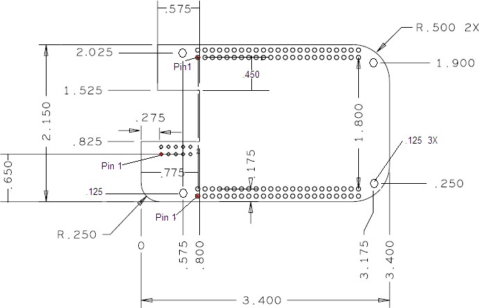
For stacking configuration, the two 46 pin expansion headers use the same connectors. Figure 66 is a picture of the connector. These are dual row 23 position 2.54mm x 2.54mm connectors.

image

Figure 66. Expansion Connector

imageimageREF: BBONEBLK_SRM BeagleBone Black System Rev C.1

___________________________________________________________________________________________________________________________________________________________________________________ *Reference Manual * The connector is mounted on the top side of the board with longer tails to allow insertion into the BeagleBone Black. *Figure 67* is the connector configuration for the connector. ___________________________________________________________________________________________________________________________________________________________________________________ image:media2/media/image153.png[image,width=564,height=54] ___________________________________________________________________________________________________________________________________________________________________________________________________________________________________________________________________________________________________________________________________________________________________________________________________________________________________________________________________________________________________________________________________________________________________________________________________________________________________________________________________________________________________________________________________________________________________________________________________________________________________ [[_bookmark219]]**Figure 67. Stacked Cape Expansion Connector** For convenience listed in *Table 18* are some possible choices for part numbers on this connector. They have varying pin lengths and some may be more suitable than others for your use. It should be noted, that the longer the pin and the further it is inserted into the BeagleBone Black connector, the harder it will be to remove due to the tension on 92 pins. This can be minimized by using shorter pins. There are most likely other suppliers out there that will work for this connector as well. If anyone finds other suppliers of compatible connectors that work, let us know and they will be added to this document. The first item in *Table 19* is on the edge and may not be the best solution. Overhang is the amount of the pin that goes past the contact point of the connector on the BeagleBone Black. The third part listed in *Table 20* will have insertion force issues. ___________________________________________________________________________________________________________________________________________________________________________________________________________________________________________________________________________________________________________________________________________________________________________________________________________________________________________________________________________________________________________________________________________________________________________________________________________________________________________________________________________________________________________________________________________________________________________________________________________________________________ [[_bookmark220]]**Table 20. Stacked Cape Connectors** [cols=",,,",options="header",] |============================================ a| __________ *SUPPLIER* __________ a| ____________ *PARTNUMBER* ____________ a| _________________ *TAIL LENGTH(in)* _________________ a| ______________ *OVERHANG(in)* ______________ a| _____________________________________________ http://www.mlelectronics.com/[_Major League_] _____________________________________________ a| __________________ SSHQ-123-D-06-G-LF __________________ a| ____ .190 ____ a| _____ 0.049 _____ a| _____________________________________________ http://www.mlelectronics.com/[_Major League_] _____________________________________________ a| __________________ SSHQ-123-D-08-G-LF __________________ a| ____ .390 ____ a| _____ 0.249 _____ a| _____________________________________________ http://www.mlelectronics.com/[_Major League_] _____________________________________________ a| __________________ SSHQ-123-D-10-G-LF __________________ a| ____ .560 ____ a| _____ 0.419 _____ |============================================ __________________________________________________________________________________________________________________________________________________________________________________________________________________________________________________________________ There are also different plating options on each of the connectors above. Gold plating on the contacts is the minimum requirement. If you choose to use a different part number for plating or availability purposes, make sure you do not select the “LT” option. Other possible sources are Sullins and Samtec but make sure you select one that has the correct mating depth. __________________________________________________________________________________________________________________________________________________________________________________________________________________________________________________________________ [[ref-bboneblk_srm-beaglebone-black-system-rev-c.1-100]] image:media2/media/image1.png[image,width=194,height=34]image:media2/media/image2.jpeg[image,width=172,height=27]REF: BBONEBLK_SRM BeagleBone Black System Rev C.1

*Reference Manual *

  1. Stacked Capes w/Signal Stealing

Figure 68 is the connector configuration for stackable capes that does not provide all of the signals upwards for use by other boards. This is useful if there is an expectation that other boards could interfere with the operation of your board by exposing those signals for expansion. This configuration consists of a combination of the stacking and non- stacking style connectors.

image

Figure 68. Stacked w/Signal Stealing Expansion Connector

  1. Retention Force

The length of the pins on the expansion header has a direct relationship to the amount of force that is used to remove a cape from the BeagleBone Black. The longer the pins extend into the connector the harder it is to remove. There is no rule that says that if longer pins are used, that the connector pins have to extend all the way into the mating connector on the BeagleBone Black, but this is controlled by the user and therefore is hard to control. We have also found that if you use gold pins, while more expensive, it makes for a smoother finish which reduces the friction.

This section will attempt to describe the tradeoffs and things to consider when selecting a connector and its pin length.

  1. BeagleBone Black Female Connectors

Figure 69 shows the key measurements used in calculating how much the pin extends past the contact point on the connector, what we call overhang.

imageimageREF: BBONEBLK_SRM BeagleBone Black System Rev C.1

___________________ *Reference Manual * ___________________ image:media2/media/image155.jpeg[image,width=552,height=312] _____________________________________________________________________________________________________________________________________________________________ [[_bookmark225]]**Figure 69. Connector Pin Insertion Depth** To calculate the amount of the pin that extends past the Point of Contact, use the following formula: Overhang=Total Pin Length- PCB thickness (.062) - contact point (.079) The longer the pin extends past the contact point, the more force it will take to insert and remove the board. Removal is a greater issue than the insertion. _____________________________________________________________________________________________________________________________________________________________ [[signal-usage]] Signal Usage ++++++++++++ _______________________________________________________________________________________________________________________________________________________________________________________________________________________________________________________________________________________________________________________________________________________________________________________________________________________________________________________ Based on the pin muxing capabilities of the processor, each expansion pin can be configured for different functions. When in the stacking mode, it will be up to the user to ensure that any conflicts are resolved between multiple stacked cards. When stacked, the first card detected will be used to set the pin muxing of each pin. This will prevent other modes from being supported on stacked cards and may result in them being inoperative. In *Section 7.1* of this document, the functions of the pins are defined as well as the pin muxing options. Refer to this section for more information on what each pin is. To simplify things, if you use the default name as the function for each pin and use those functions, it will simplify board design and reduce conflicts with other boards. Interoperability is up to the board suppliers and the user. This specification does not specify a fixed function on any pin and any pin can be used to the full extent of the functionality of that pin as enabled by the processor. _______________________________________________________________________________________________________________________________________________________________________________________________________________________________________________________________________________________________________________________________________________________________________________________________________________________________________________________ [[ref-bboneblk_srm-beaglebone-black-system-rev-c.1-102]] image:media2/media/image1.png[image,width=194,height=34]image:media2/media/image2.jpeg[image,width=172,height=27]REF: BBONEBLK_SRM BeagleBone Black System Rev C.1

*Reference Manual *

DO NOT APPLY VOLTAGE TO ANY I/O PIN WHEN POWER IS NOT SUPPLIED TO THE BOARD. IT WILL DAMAGE THE PROCESSOR AND VOID THE WARRANTY.

NO PINS ARE TO BE DRIVEN UNTIL AFTER THE SYS_RESET LINE GOES HIGH.

Cape Power

This section describes the power rails for the capes and their usage.

  1. Main Board Power

The Table 1 describes the voltages from the main board that are available on the expansion connectors and their ratings. All voltages are supplied by connector P9. The current ratings listed are per pin.

Table 21. Expansion Voltages

Current Name _ P9 _ Name Current _ GND _

1

_ 2 _


GND _

250mA

VDD_3V3B

3

_ 4 _

VDD_3V3B

250mA

1000mA

VDD_5V

5

_ 6 _

VDD_5V

1000mA

250mA

SYS_5V

7

_ 8 _

SYS_5V

250mA

:

_ : _


GND _

43

44


GND _


GND _

The VDD_3V3B rail is supplied by the LDO on the BeagleBone Black and is the primary power rail for expansion boards. If the power requirement for the capes exceeds the current rating, then locally generated voltage rail can be used. It is recommended that this rail be used to power any buffers or level translators that may be used.

VDD_5V is the main power supply from the DC input jack. This voltage is not present when the board is powered via USB. The amount of current supplied by this rail is dependent upon the amount of current available. Based on the board design, this rail is limited to 1A per pin from the main board.

The SYS_5V rail is the main rail for the regulators on the main board. When powered from a DC supply or USB, this rail will be 5V. The available current from this rail depends on the current available from the USB and DC external supplies.

  1. Expansion Board External Power

imageimageREF: BBONEBLK_SRM BeagleBone Black System Rev C.1

__________________________________________________________________________________________________________________________________________________________________________________________________________________________________________________________________________________________________________________________________________________________________ *Reference Manual * A cape can have a jack or terminals to bring in whatever voltages may be needed by that board. Care should be taken not to let this voltage be fed back into any of the expansion header pins. It is possible to provide 5V to the main board from an expansion board. By supplying a 5V signal into the *VDD_5V* rail, the main board can be supplied. This voltage must not exceed 5V. You should not supply any voltage into any other pin of the expansion connectors. Based on the board design, this rail is limited to 1A per pin to the BeagleBone Black. *There are several precautions that need to me taken when working with the expansion headers to prevent damage to the board.* __________________________________________________________________________________________________________________________________________________________________________________________________________________________________________________________________________________________________________________________________________________________________ 1. *Do not apply any voltages to any I/O pins when the board is not powered on.* 2. *Do not drive any external signals into the I/O pins until after the VDD_3V3B rail is up.* 3. *Do not apply any voltages that are generated from external sources.* 4. *If voltages are generated from the VDD_5V signal, those supplies must not become active until after the VDD_3V3B rail is up.* 5. *If you are applying signals from other boards into the expansion headers, make sure you power the board up after you power up the BeagleBone Black or make the connections after power is applied on both boards.* ____________________________________________________________________________ *Powering the processor via its I/O pins can cause damage to the processor.* ____________________________________________________________________________ [[mechanical]] Mechanical ++++++++++ _____________________________________________________________________________________________________________________________________________________________________________________________________________________________________________________________________________________________________________________________________________________________________________________________________________________________________ This section provides the guidelines for the creation of expansion boards from a mechanical standpoint. Defined is a standard board size that is the same profile as the BeagleBone Black. It is expected that the majority of expansion boards created will be of standard size. It is possible to create boards of other sizes and in some cases this is required, as in the case of an LCD larger than the BeagleBone Black board. _____________________________________________________________________________________________________________________________________________________________________________________________________________________________________________________________________________________________________________________________________________________________________________________________________________________________________ 1. [[_bookmark232]][[bookmark232]]**Standard Cape Size** ______________________________________________________________________________ *Figure 70* is the outline of the standard cape. The dimensions are in inches. ______________________________________________________________________________ [[ref-bboneblk_srm-beaglebone-black-system-rev-c.1-104]] image:media2/media/image1.png[image,width=194,height=34]image:media2/media/image2.jpeg[image,width=172,height=27]REF: BBONEBLK_SRM BeagleBone Black System Rev C.1

*Reference Manual *

image

Figure 70. Cape Board Dimensions

A slot is provided for the Ethernet connector to stick up higher than the cape when mounted. This also acts as a key function to ensure that the cape is oriented correctly. Space is also provided to allow access to the user LEDs and reset button on the main board.

Some people have inquired as to the difference in the radius of the corners of the BeagleBone Black and why they are different. This is a result of having the BeagleBone fit into the Altoids style tin.

It is not required that the cape be exactly like the BeagleBone Black board in this respect.

  1. Extended Cape Size

Capes larger than the standard board size are also allowed. A good example would be an LCD panel. There is no practical limit to the sizes of these types of boards. The notch for the key is also not required, but it is up to the supplier of these boards to ensure that the BeagleBone Black is not plugged in incorrectly in such a manner that damage would be cause to the BeagleBone Black or any other capes that may be installed. Any such damage will be the responsibility of the supplier of such a cape to repair.

As with all capes, the EEPROM is required and compliance with the power requirements must be adhered to.

imageimageREF: BBONEBLK_SRM BeagleBone Black System Rev C.1

___________________ *Reference Manual * ___________________ 1. [[_bookmark235]][[bookmark235]]**Enclosures** _______________________________________________________________________________________________________________________________________________________________________________________________________________________________________________________________________________________________________________________ There are numerous enclosures being created in all different sizes and styles. The mechanical design of these enclosures is not being defined by this specification. The ability of these designs to handle all shapes and sizes of capes, especially when you consider up to four can be mounted with all sorts of interface connectors, it is difficult to define a standard enclosure that will handle all capes already made and those yet to be defined. If cape designers want to work together and align with one enclosure and work around it that is certainly acceptable. But we will not pick winners and we will not do anything that impedes the openness of the platform and the ability of enclosure designers and cape designers to innovate and create new concepts. _______________________________________________________________________________________________________________________________________________________________________________________________________________________________________________________________________________________________________________________ [[ref-bboneblk_srm-beaglebone-black-system-rev-c.1-106]] image:media2/media/image1.png[image,width=194,height=34]image:media2/media/image2.jpeg[image,width=172,height=27]REF: BBONEBLK_SRM BeagleBone Black System Rev C.1

*Reference Manual *

  1. BeagleBone Black Mechanical ^^^^^^^^^

  2. Dimensions and Weight

____________________________________________________________________________________________________________________________________________________________________ Size: 3.5” x 2.15” (86.36mm x 53.34mm) Max height: .187” (4.76mm) PCB Layers: 6 PCB thickness: .062” RoHS Compliant: Yes Weight: 1.4 oz image:media2/media/image1.png[image,width=194,height=34]image:media2/media/image2.jpeg[image,width=172,height=27]*REF: BBONEBLK_SRM BeagleBone Black System Rev C.1* *Reference Manual * ____________________________________________________________________________________________________________________________________________________________________ [[silkscreen-and-component-locations]] image:media2/media/image157.png[image,width=518,height=771]Silkscreen and Component Locations +++++++++++++++++++++++++++++++++++++++++++++++++++++++++++++++++++++++++++++++++++++++++++++ _______________________________________________ [[_bookmark239]]**Figure 71. Board Dimensions** _______________________________________________ [[ref-bboneblk_srm-beaglebone-black-system-rev-c.1-107]] image:media2/media/image1.png[image,width=194,height=34]image:media2/media/image2.jpeg[image,width=172,height=27]REF: BBONEBLK_SRM BeagleBone Black System Rev C.1 ++++++++++++++++++++++++++++++++++++++++++++++++++++++++++++++++++++++++++++++++++++++++++++++++++++++++++++++++++++++++++++++++++++++++++++++++++++++++++++++++++ ___________________ *Reference Manual * ___________________ image:media2/media/image158.jpeg[image,width=486,height=792] ________________________________________________________ [[_bookmark240]]**Figure 72. Component Side Silkscreen** ________________________________________________________ [[ref-bboneblk_srm-beaglebone-black-system-rev-c.1-108]] image:media2/media/image1.png[image,width=194,height=34]image:media2/media/image2.jpeg[image,width=172,height=27]REF: BBONEBLK_SRM BeagleBone Black System Rev C.1 ++++++++++++++++++++++++++++++++++++++++++++++++++++++++++++++++++++++++++++++++++++++++++++++++++++++++++++++++++++++++++++++++++++++++++++++++++++++++++++++++++ ___________________ *Reference Manual * ___________________ image:media2/media/image159.png[image,width=494,height=771] ______________________________________________________ [[_bookmark241]]**Figure 73. Circuit Side Silkscreen** ______________________________________________________ [[ref-bboneblk_srm-beaglebone-black-system-rev-c.1-109]] image:media2/media/image1.png[image,width=194,height=34]image:media2/media/image2.jpeg[image,width=172,height=27]REF: BBONEBLK_SRM BeagleBone Black System Rev C.1 ++++++++++++++++++++++++++++++++++++++++++++++++++++++++++++++++++++++++++++++++++++++++++++++++++++++++++++++++++++++++++++++++++++++++++++++++++++++++++++++++++ ___________________________________________________________________________________________ *Reference Manual * image:media2/media/image160.jpeg[image,width=476,height=768][[_bookmark242]]*10.0 Pictures* [[_bookmark243]]**Figure 74. Top Side** ___________________________________________________________________________________________ [[ref-bboneblk_srm-beaglebone-black-system-rev-c.1-110]] image:media2/media/image1.png[image,width=194,height=34]image:media2/media/image2.jpeg[image,width=172,height=27]REF: BBONEBLK_SRM BeagleBone Black System Rev C.1 ++++++++++++++++++++++++++++++++++++++++++++++++++++++++++++++++++++++++++++++++++++++++++++++++++++++++++++++++++++++++++++++++++++++++++++++++++++++++++++++++++ ___________________ *Reference Manual * ___________________ image:media2/media/image161.jpeg[image,width=486,height=764] __________________________________________ [[_bookmark244]]**Figure 75. Bottom Side** __________________________________________ [[ref-bboneblk_srm-beaglebone-black-system-rev-c.1-111]] image:media2/media/image1.png[image,width=194,height=34]image:media2/media/image2.jpeg[image,width=172,height=27]REF: BBONEBLK_SRM BeagleBone Black System Rev C.1 ++++++++++++++++++++++++++++++++++++++++++++++++++++++++++++++++++++++++++++++++++++++++++++++++++++++++++++++++++++++++++++++++++++++++++++++++++++++++++++++++++ ___________________ *Reference Manual * ___________________ [[support-information]] Support Information ^^^^^^^^^^^^^^^^^^^ ____________________________________________________________________________________________________________________________________________ All support for this design is through the BeagleBoard.org community at: mailto:beagleboard@googlegroups.com[_beagleboard@googlegroups.com_] or http://beagleboard.org/discuss[_http://beagleboard.org/discuss_] . ____________________________________________________________________________________________________________________________________________ [[hardware-design]] Hardware Design +++++++++++++++ ________________________________________________________________________________________________________________________________________________________ Design documentation can be found on the eMMC of the board under the documents/hardware directory when connected using the USB cable. Provided there is: ________________________________________________________________________________________________________________________________________________________ * Schematic in PDF * Schematic in OrCAD (Cadence Design Entry CIS 16.3) * PCB Gerber * PCB Layout File (Allegro) * Bill of Material * System Reference Manual (This document). ______________________________________________________________________________________________________________________________________________________________________________________________________________________________________________________________________________________________________________________________________________________________________________________________________ This directory is not always kept up to date in every SW release due to the frequency of changes of the SW. The best solution is to download the files from the Circuitco WIKI at http://circuitco.com/support/index.php?title=BeagleBoneBlack[_http://circuitco.com/support/index.php?title=BeagleBoneBlack_] We do not track SW revision of what is in the eMMC. SW is tracked separately from the HW due to the frequency of changes which would require massive relabeling of boards due to the frequent SW changes. You should always use the latest SW revision. To see what SW revision is loaded into the eMMC follow the instructions at http://circuitco.com/support/index.php?title=Updating_The_Software&Checking_The_Angstrom_Image_Version[_http://circuitco.com/support/index.php?title=Updating_The_Software#Checking_The_An_] http://circuitco.com/support/index.php?title=Updating_The_Software&Checking_The_Angstrom_Image_Version[_gstrom_Image_Version_] ______________________________________________________________________________________________________________________________________________________________________________________________________________________________________________________________________________________________________________________________________________________________________________________________________ [[software-updates]] Software Updates ++++++++++++++++ ______________________________________________________________________________________________________________________________________________________________________________________________________________________________________________________________________________ It is a good idea to always use the latest software. Instructions for how to update your software to the latest version can be found at: http://circuitco.com/support/index.php?title=BeagleBoneBlack&Updating_the_eMMC_Software[_http://circuitco.com/support/index.php?title=BeagleBoneBlack#Updating_the_eMMC_S_] http://circuitco.com/support/index.php?title=BeagleBoneBlack&Updating_the_eMMC_Software[_oftware_] ______________________________________________________________________________________________________________________________________________________________________________________________________________________________________________________________________________ [[ref-bboneblk_srm-beaglebone-black-system-rev-c.1-112]] image:media2/media/image1.png[image,width=194,height=34]image:media2/media/image2.jpeg[image,width=172,height=27]REF: BBONEBLK_SRM BeagleBone Black System Rev C.1 ++++++++++++++++++++++++++++++++++++++++++++++++++++++++++++++++++++++++++++++++++++++++++++++++++++++++++++++++++++++++++++++++++++++++++++++++++++++++++++++++++ ___________________ *Reference Manual * ___________________ [[rma-support]] RMA Support +++++++++++ __________________________________________________________________________________________________________________________________________________________________________________________________________________________________________________________________________________________________________________________________________________________________________________________________________________________________________________ If you feel your board is defective or has issues, request an RMA by filling out the form at http://beagleboard.org/support/rma[_http://beagleboard.org/support/rma_] . You will need the serial number and revision of the board. The serial numbers and revisions keep moving. Different boards can have different locations depending on when they were made. The following figures show the three locations of the serial and revision number. __________________________________________________________________________________________________________________________________________________________________________________________________________________________________________________________________________________________________________________________________________________________________________________________________________________________________________________ image:media2/media/image162.jpeg[image,width=517,height=308] ___________________________________________________________________________ [[_bookmark249]]**Figure 76. Initial Serial Number and Revision Locations** ___________________________________________________________________________ image:media2/media/image163.jpeg[image,width=521,height=232] _______________________________________________________________________________ [[_bookmark250]]**Figure 77. Second Phase Serial Number and Revision Location** _______________________________________________________________________________ [[ref-bboneblk_srm-beaglebone-black-system-rev-c.1-113]] image:media2/media/image1.png[image,width=194,height=34]image:media2/media/image2.jpeg[image,width=172,height=27]REF: BBONEBLK_SRM BeagleBone Black System Rev C.1 ++++++++++++++++++++++++++++++++++++++++++++++++++++++++++++++++++++++++++++++++++++++++++++++++++++++++++++++++++++++++++++++++++++++++++++++++++++++++++++++++++ ___________________ *Reference Manual * ___________________ image:media2/media/image164.jpeg[image,width=573,height=221] ______________________________________________________________________________ [[_bookmark251]]**Figure 78. Third Phase Serial Number and Revision Location** ______________________________________________________________________________ [[trouble-shooting-hdmi-issues]] Trouble Shooting HDMI Issues ++++++++++++++++++++++++++++ ________________________________________________________________________________________________________________________________________________________________________________________________________________________________________________________________________________________________________________________________________________________________________________________________________________________________________________________________________________________________________________________________________________________________________________________________ Many people are having issues with getting HDMI to work on their TV/Display. Unfortunately, we do not have the resources to buy all the TVs and Monitors on the market today nor go to eBay and buy all of the TVs and monitors made over the last five years to thoroughly test each and every one. We are depending on community members to help us get these tested and information provided on how to get them to work. One would think that if it worked on a lot of different TVs and monitors it would work on most if not all of them, assuming they meet the specification. However, there are other issues that could also result in these various TVs and monitors not working. The intent is that this page will be useful in navigating some of these issues. As others also find solutions, as long as we know about them, they will be added here as well. For access to the most up to date troubleshooting capabilities, go to the support wiki at _http://www.elinux.org/Beagleboard:BeagleBoneBlack_HDMI_ The early release of the Software had some issues in the HDMI driver. Be sure and use the latest SW to take advantage of the improvements. _http://www.elinux.org/Beagleboard:BeagleBoneBlack#Software_Resources_ ________________________________________________________________________________________________________________________________________________________________________________________________________________________________________________________________________________________________________________________________________________________________________________________________________________________________________________________________________________________________________________________________________________________________________________________________ 1. [[_bookmark253]][[bookmark253]]**EDID** _______________________________________________________________________________________________________________________________________________________________________________________________________________________________________________________________________________________________________________________________________________________________________________________________________________________________________________________________________________________ EDID is the way the board requests information from the display and determines all the resolutions that it can support. The driver on the board will then look at these timings and find the highest resolution that is compatible with the board and uses that resolution for the display. For more information on EDID, you can take a look at http://en.wikipedia.org/wiki/Extended_display_identification_data[_http://en.wikipedia.org/wiki/Extended_display_identification_data_] _______________________________________________________________________________________________________________________________________________________________________________________________________________________________________________________________________________________________________________________________________________________________________________________________________________________________________________________________________________________ [[ref-bboneblk_srm-beaglebone-black-system-rev-c.1-114]] image:media2/media/image1.png[image,width=194,height=34]image:media2/media/image2.jpeg[image,width=172,height=27]REF: BBONEBLK_SRM BeagleBone Black System Rev C.1 ++++++++++++++++++++++++++++++++++++++++++++++++++++++++++++++++++++++++++++++++++++++++++++++++++++++++++++++++++++++++++++++++++++++++++++++++++++++++++++++++++ [[reference-manual-3]] Reference Manual ++++++++++++++++++ _______________________________________________________________________________________________________________________________________ If the board is not able to read the EDID, for whatever reason, it does not have this information. A few possible reasons for this are: _______________________________________________________________________________________________________________________________________ * Bad cable * Cable not plugged in all the way on both ends * Display not powered on. (It should still work powered off, but some displays do not). 1. [[_bookmark254]][[bookmark254]]**DISPLAY SOURCE SELECTION** __________________________________________________________________________________________________________________________________________________________________________________________________________________________________________________________ One easy thing to overlook is that you need to select the display source that matches the port you are using on the TV. Some displays may auto select, so you may need to disconnect the other inputs until you are sure the display works with the board. __________________________________________________________________________________________________________________________________________________________________________________________________________________________________________________________ 1. [[_bookmark255]][[bookmark255]]**OUT OF SEQUENCE** ________________________________________________________________________________________________________________________________________________________________________________________________________________________________________________________________________ Sometimes the display and the board can get confused. One way to prevent this is after everything is cabled up and running, you can power cycle the display, with the board still running. You can also try resetting the board and let it reboot to resync with the TV. ________________________________________________________________________________________________________________________________________________________________________________________________________________________________________________________________________ 1. [[_bookmark256]][[bookmark256]]**OVERSCAN** ________________________________________________________________________________________________________________________________________________________________________________________________________________________________________________ Some displays use what is called overscan. This can be seen in TVs and not so much on Monitors. It causes the image to be missing on the edges, such that you cannot see them displayed. Some higher end displays allow you to disable overscan. Most TVs have a mode that allows you to adjust the image. These are options like Normal, Wide, Zoom, or Fit. Normal seems to be the best option as it does not chop of the edges. The other ones will crop of the edges. ________________________________________________________________________________________________________________________________________________________________________________________________________________________________________________ 1. [[_bookmark257]][[bookmark257]]**Taking a Nap** ________________________________________________________________________________________________________________________________________________________________________________________________________________________________________________________________________ In some cases the board can come up in a power down/screen save mode. No display will be present. This is due to the board believing that it is asleep. To come out of this, you will need to hit the keyboard or move the mouse. Once working, the board will time out and go back to sleep again. This can cause the display to go into a power down mode as well. You may need to turn the display back on again. Sometimes, it may take a minute or so for the display to catch up and show the image. ________________________________________________________________________________________________________________________________________________________________________________________________________________________________________________________________________ 1. [[_bookmark258]][[bookmark258]]**AUDIO** _________________________________________________________________________________________________________________________________________________________________________________ Audio will only work on TV resolutions. This is due to the the way the specification was written. Some displays have built in speakers and others require external. Make sure you _________________________________________________________________________________________________________________________________________________________________________________ [[ref-bboneblk_srm-beaglebone-black-system-rev-c.1-115]] image:media2/media/image1.png[image,width=194,height=34]image:media2/media/image2.jpeg[image,width=172,height=27]REF: BBONEBLK_SRM BeagleBone Black System Rev C.1 ++++++++++++++++++++++++++++++++++++++++++++++++++++++++++++++++++++++++++++++++++++++++++++++++++++++++++++++++++++++++++++++++++++++++++++++++++++++++++++++++++ __________________________________________________________________________________________________________________________________________________________________________________________________________________ *Reference Manual * have a TV resolution and speakers are connected if they are not built in. The SW should default to a TV resolution giving audio support. The HDMI driver should default to the highest audio supported resolution. __________________________________________________________________________________________________________________________________________________________________________________________________________________ 1. [[_bookmark259]][[bookmark259]]**Getting Help** _______________________________________________________________________________________________________________________________________________________________________________________________________________________ If you need some up to date troubleshooting techniques, we have a Wiki set up at http://circuitco.com/support/index.php?title=BeagleBoneBlack_HDMI[_http://circuitco.com/support/index.php?title=BeagleBoneBlack_HDMI_] _______________________________________________________________________________________________________________________________________________________________________________________________________________________