Component and PCell Layout
This page describes the requirements for creating components that are recognized by SiEPIC-Tools, to enable the functionality of waveguide snapping, component snapping, verification, netlist extraction, and simulation.
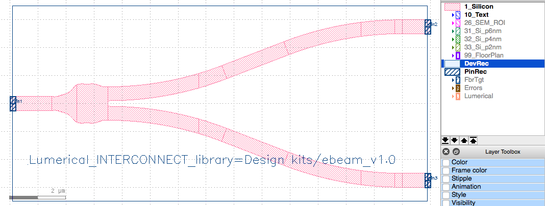
Here is an example component with all the necessary DevRec and PinRec marking shapes and text labels. These are necessary to enable the circuit verification and netlist extraction for simulations.
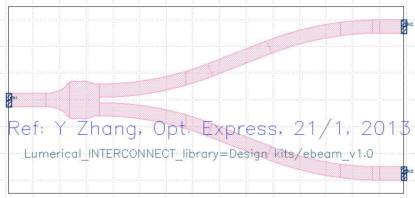
The purposes of the DevRec and PinRec layers are to:
-
enable interactive waveguide routing. Components and pins are recognized via geometries contained within a DevRec polygon. A database is created by scanning the GDS and making a list of all components that can be routed to.
-
enable Lumerical INTERCONNECT circuit simulations. DevRec defines the extent of the photonic component. For example, a YBranch has 3 optical input/outputs (defined via the PinRec) and is surrounded by DevRec. In Lumerical FDTD simulations, we can convert the DevRec into a simulation boundary condition (e.g., PML) and generate S-Parameters by placing the simulation Ports to be located where the pins are placed (PinRec).
The DevRec layer is also used for verification:
- Components should not be overlapping, as enforced by a rule that checks that there are no overlapping DevRec layers. This prevents devices from being too close causing optical cross-talk. For example, two waveguides brought close together would cause parasitic coupling. The DevRec should thus be drawn far enough away from the device, at a point where the optical fields have decayed sufficiently so that when two components are placed side by side, they do not couple. For TE 1550 nm strip waveguides, 500-1000 nm may be sufficiently far.
-
Shapes to be fabricated, drawn on silicon layer
-
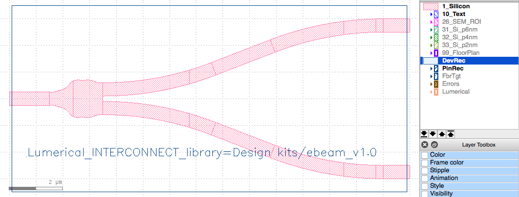
Device Recognition layer – DevRec. We need two shapes:
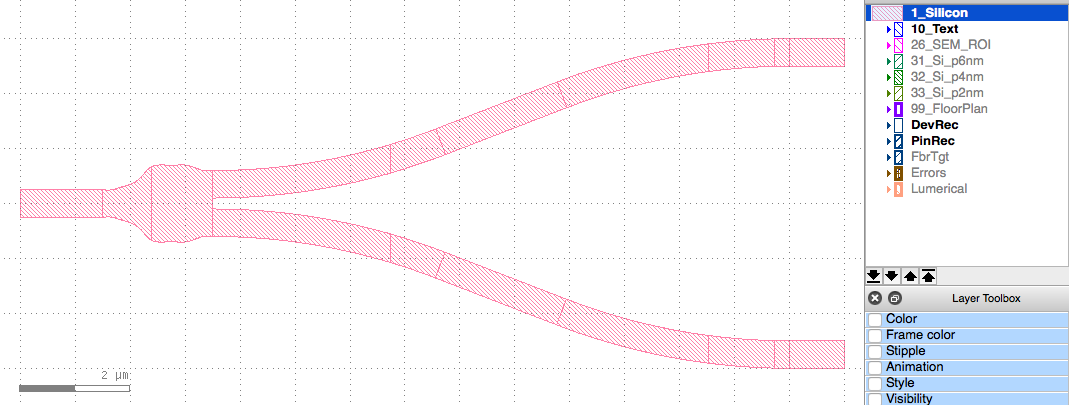
- A Box or Polygon shape surrounding the component.
- A Text shape, providing a path to the Lumerical INTERCONNECT model library:
Lumerical_INTERCONNECT_library=xxx, where xxx is the name of the Compact Model Library. - A Text shape, providing a component name that matches the component name in the library:
Component=xxxwhere xxx is the name of the element in the Compact Model Library. - Parameterized Cells (PCell) parameters - Spice format:
A Text shape, such as
Spice_param=wg_width=0.5e-6 gap=2e-6.
-
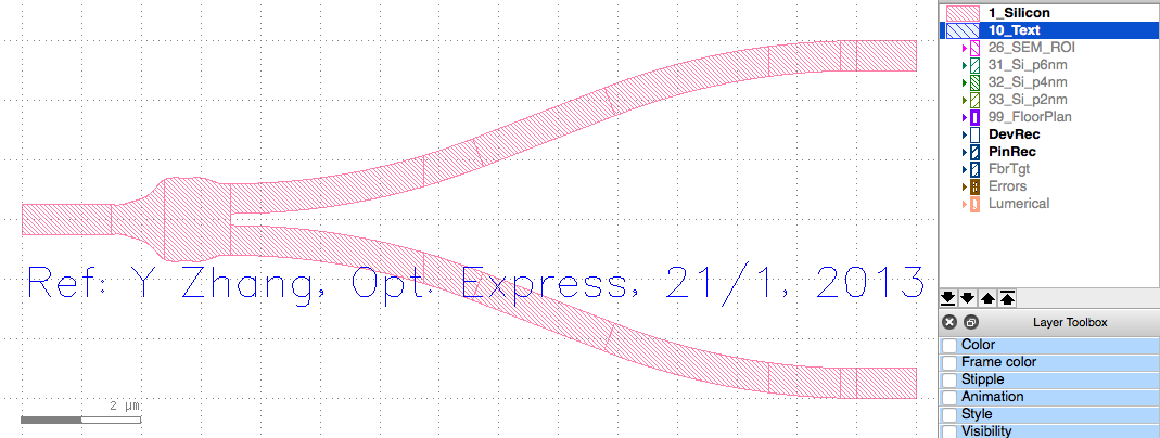
Text description of this component. Ideally a journal paper reference. Placed on the Text layer.
-
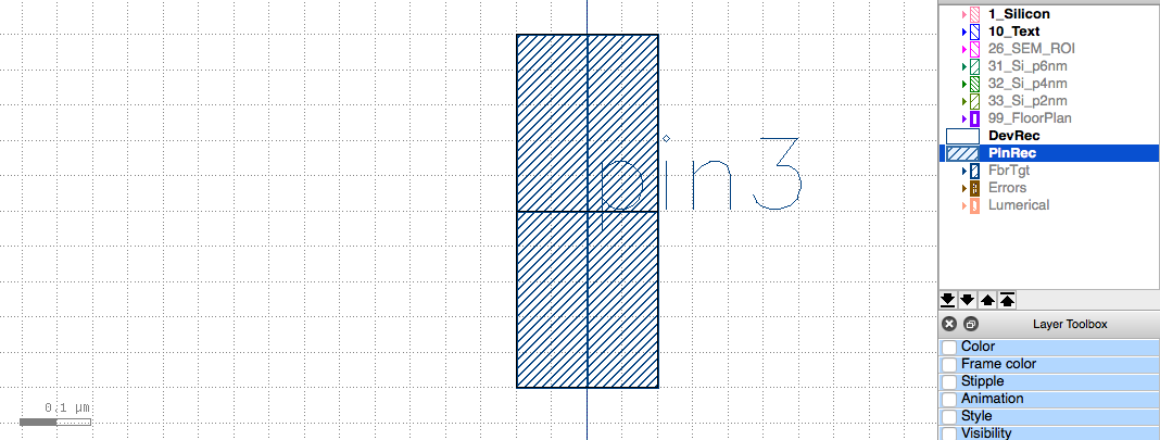
OPTICAL PINS - Pin Recognition layer - PinRec. We need two shapes:
- A Path shape (only) identifying the pin. The waveguide will be snapped to the path, and at the mid-point. Do not use a Polygon or a Box for this. The Path is necessary since a) it provides information on the direction the waveguide must go, b) it makes it very easy to detect offset pin-to-waveguide connections and width mismatches. The Path is used to identify it as an optical pin.
- The pin directions in all components must be consistent so that we can identify which pins can connect to with other ones. By convention, we define that the path indicates which way the signal is LEAVING the component (path starts with the point inside the DevRec, with the second point outside).
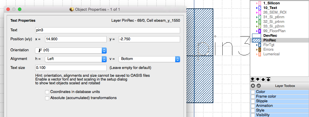
- A Text shape, with the name of the pin. It must be located exactly in the mid-point of the Path shape. Note that we require that the pin text label be at the midpoint of the path.
Notes:
- The waveguide should be straight at the pin. A pin that features a curved or tapered waveguide means that the performance of the component will change depending on what it is connected to.
- The waveguide should overlap completely with the PinRec. This allows DRC checking to compare the PinRec and waveguide layers, and is used to detect waveguide disconnects, waveguide pin width mismatches, and waveguide material mismatches.
We recommend having the DevRec crossing through the same midpoints of all pins.
- The pins are exported in the netlist in alphabetical order. The pin order must match the port order in the Lumerical Compact Model Library (CML). If you cannot achieve this with alphabetical ordering alone, then you can enforce explicit ordering by adding a number to the beginning of the pin names, as follows: 01_xxx, 02_xxx, .... NN_xxx. Note that all pins must be numbered (including electrical) in order for explicit ordering to work.

- ELECTRICAL PINS - Pin Recognition layer - PinRecM. We need two shapes:
- A Path shape (only) identifying the pin. The Path is used to identify it as an electrical pin with a direction (same as optical pin).
- A Text shape, with the name of the pin. It must be located inside the Box shape. The pins are exported in the netlist by alphabetical order, or they can be explicitly numbered (01_xxx, 02_xxx, .... NN_xxx) to match the Lumerical Compact Model Library (CML).
- OPTICAL IO PINS - Optical fibre target layer - FbrTgt. We need:
- A Polygon shape (only) identifying the pin. The Polygon on the FbrTgt layer is used to identify it as an optical pin, and is typically a circle representing the size of the optical beam.
- A Text shape, with the name of the pin; located inside the Polygon shape.
Hierarchy is permissible, however, all the DevRec and PinRec shapes must be in the component top cell.
PCells are defined using KLayout's standard PCell format. See the KLayout Macro Templates, PCell Template.
SiEPIC-Tools provides additional functionality:
- The PCell can have a drop-down menu of a Waveguide from the Technology:
  def __init__(self):
    super(wg_heater, self).__init__()
    from SiEPIC.utils import get_technology_by_name, load_Waveguides_by_Tech
    self.technology_name = 'EBeam'
    TECHNOLOGY = get_technology_by_name(self.technology_name)
    # Load all waveguides
    self.waveguide_types = load_Waveguides_by_Tech(self.technology_name)
    p = self.param("waveguide_type", self.TypeList, "Waveguide Type", default = self.waveguide_types[0]['name'])
    for wa in self.waveguide_types:
        p.add_choice(wa['name'],wa['name'])
- PinRec, PinRecM, DevRec are available as layers:
    self.param("pinrec", self.TypeLayer, "PinRec Layer", default = TECHNOLOGY['PinRec'])
    self.param("devrec", self.TypeLayer, "DevRec Layer", default = TECHNOLOGY['DevRec'])
    self.param("pinrecm", self.TypeLayer, "PinRecM Layer (metal)", default=TECHNOLOGY['PinRecM'])
- There is a function that creates the Pins:
    from SiEPIC.utils.layout import make_pin
    LayerPinRecM = self.layout.layer(self.pinrecm)
    make_pin(self.cell, "elec1", [self.metal_width / 2, self.mh_width/2], ml_width, LayerPinRecM, 90)
Units: input can be float for microns, or int for nm
- Automated generation of DevRec and PinRec layers.
- Menu item SiEPIC > Layout > Make SiEPIC Component from cell.
- First select a cell
- Then specify on which sides the ports should appear