SiEPIC Tools Menu descriptions
Waveguide types are defined within each PDK, specific to each technology, in a WAVEGUIDES.xml file. Users may add additional waveguide types by creating a WAVEGUIDES_custom.xml file (all WAVEGUIDES_*.xml files are loaded). Examples of waveguide specification files: WAVEGUIDES.xml for EBeam and WAVEGUIDES.xml for GSiP
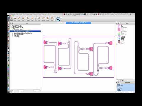
To create a waveguide:
-
draw a Path on the waveguide layer
-
hotkey "W", or menu SiEPIC | Waveguides | Path to Waveguide
-
This brings up a set of choices, which are specified in the WAVEGUIDES.xml file, specific to each technology.
-
Configuration drop-down: one of the pre-configured waveguide types. Choosing one changes the parameters in the Bend Specifications.
-
Bend Specifications:
-
Radius: as defined to the middle of the waveguide.
-
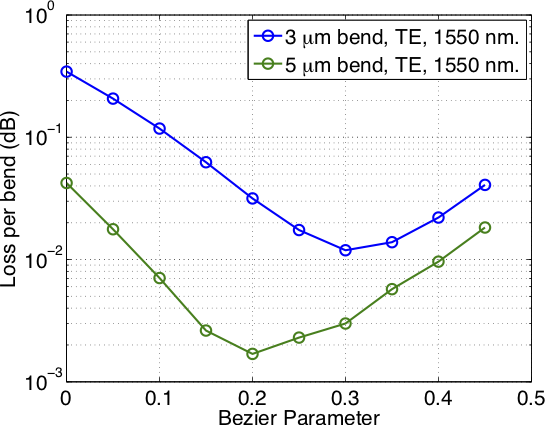
Bezier Parameter for adiabatic bends: when unselected, the bend is a circle corner; selected allows for optimized adiabatic bends. The following is a simulation result for TE 1550 nm strip waveguides with dimensions of 500 x 220 nm:
-
-
Examples of scripted layout implementation.
Design for Manufacturing (DFM) checking can be performed using Mentor Calibre, running on an external Linux server. Typically a foundry provides a set of design rules in a DRC file, containing: minimum feature size, minimum feature spacing, inclusion and exclusion rules, and pattern density requirements.
Functional design verification is implemented in SiEPIC-Tools and includes:
-
Waveguide checking
- Waveguide path: Only 2 points allowed in a path. Convert to a Waveguide if necessary.
- Radius: Not enough space to accommodate the desired bend radius for the waveguide.
- Bend points: Waveguide bend should have a sufficient number of points per circle.
- Manhattan: The first and last waveguide segment need to be Manhattan (vertical or horizontal) so that they can connect to device pins.
-
Component checking
- Flattened component: SiEPIC-Tools Verification, Netlist extraction, and Simulation only function on hierarchical layouts, and not on flattened layouts.
- Overlapping component: defined as overlapping DevRec layers; touching is ok.
-
Connectivity checking
- Disconnected pin: all component pins should be connected to other components or waveguides. Connectivity must be perfect, with the pins facing each other with the same angle (180 degrees), and with the same position (accurate to the user database unit).
- Mismatched pin widths: the waveguides need to be the same dimension (width) and type (e.g., strip versus rib)
-
Simulation checking
- Missing compact model: Compact model are required for all components to perform simulations. Possible reasons: 1) Please run SiEPIC | Simulation | Setup Lumerical INTERCONNECT and CML, to make sure that the Compact Model Library is installed in INTERCONNECT, and that KLayout has a list of all component models. 2) the library does not have a compact model for this component.
-
Design for Test checking: These parameters are specified in the DFT.xml file, specific to each technology. DFT.xml for EBeam and DFT.xml for GSiP
-
Implemented using Python functions, rather than the KLayout DRC script language. Allows for more complex rule creation, including loading parameters from XML files. Existing code can be adjusted for different parameters, or modified and extended to deal with different DFT constraints (e.g., Design for Packaging constraints for bond pad locations and pitch). Default DFT code is for automated testing (e.g., using a MapleLeaf Photonics automated silicon photonics probe station) with fibre arrays aligned to vertical grating couplers. Could be adjusted for edge coupling and electrical test.
-
opt_in label required: Automated test opt_in labels are used to generate the test vectors for automated measurements. Labels must be on the layer "Text", and formatted as
- opt_in_{polarization}_{wavelength}_{type}_{deviceID}_{parameters}, where polarization and wavelength are defined in DFT.xml, e.g., TE and 1550; type is for the automated probe station to know what type of device is being measured, e.g., "device", deviceID is a user specific device name, and parameters are optional fields for the user.
-
opt_in label uniqueness: Automated test opt_in labels should be unique.
-
opt_in label location: Automated test opt_in labels must be placed near the tip of the grating coupler, namely near the (0,0) point of the cell.
-
opt_in wavelength: check if the wavelength is defined in the DFT.xml file
-
opt_in polarization: check if the wavelength is defined in the DFT.xml file
-
Grating Coupler pitch: Grating couplers must be on a X micron pitch, vertically arranged. X is specific to the technology, and is 127 microns for the edX course with EBeam fabrication.
-
Grating coupler orientation: The grating coupler is not oriented (rotated) the correct way for automated testing. In the edX course with EBeam fabrication, we use 0 degrees (tip pointing to the right) for the ebeam_gc_te1550 and 180 degrees (tip pointing to the left) for the ebeam_gc_tm1550.
-
Fibre array configuration: Circuit must be connected such that there is at most X Grating Couplers above the opt_in label (laser injection port) and at most Y Grating Couplers below the opt_in label. X=1 and Y=2 for the edX course with EBeam fabrication
-
- Configure the system path environment variable so that KLayout can find Lumerical tools (requires a restart of KLayout)
- Run Lumerical INTERCONNECT tool to check it works
- Load the Lumerical Python API
- Install the Compact Model Library (CML) for the presently active Technology
- Get a list of all components in the CMLs so that KLayout can perform verification checks later
- Check if all components in the present layout have associated Compact Models in Lumerical INTERCONNECT. Do this before running a simulation.
- Export the present layout as a netlist, and simulate the circuit. Requires a Laser and detector to be included in the layout, or opt_in labels to generate the test vector, e.g., for a MapleLeaf Photonics automated silicon photonics probe station.
- Same as above, except perform several simulations, taking into account the correlations due to the layout
- Repeat a simulation after you change the parameters
- Perform a simulation for the selected component. User chooses which pin to inject light into, and INTERCONNECT will plot the component response versus wavelength for all the ports.
Summary:
- run FDTD simulations and generate S-Parameters for a component.
- Presently works for a single layer, reading only geometries from the "Waveguide" layer
Usage:
- select a component, then run the menu item
This function does the following:
-
reads the file FDTD.xml to configure the fabrication process and simulation parameters
- one for each technology, located anywhere in the respective "tech" folder. You can edit this file using an external editor to configure the default parameters. If the technology is installed via the Package Manager, note that the file will get over-written the next time the package is updated.
-
present a GUI letting the user change the FDTD parameters. Some of the parameters that need more explanation:
- mode_selection: "1" = TE, "2" = TM, "1,2" = TE and TM. Presently TM doesn't work correctly.
- convergence_tests: 1 = True, 0 = False. This performs rapid FDTD simulations with a sweep of the simulation boundary to make sure it is large enough. This is particularly important for sub-wavelength grating devices, where the mode source may be in the strip waveguide and highly confined, but the light propagating in the device has a large mode area (low effective index), hence requires a much larger simulation region.
- mesh_accuracy: value from 1 to 8. 1 is a fast simulation to verify that everything is working. 3 or 4 is typically sufficiently accurate.
- Perform-quick-corner-analysis: perform simulations of the process corners at the beginning to help study anticipate variability.
- Perform-final-corner-analysis: creates a model that is suitable for Monte Carlo simulations.
-
auto-export the layout (as polygons) for the selected device.
-
configure FDTD using Component and Pin information; FDTD Ports with correct direction, polarization (single mode, or simulate for multiple modes).
-
run a single simulation: user can verify it is working
-
perform convergence testing on Z-span
-
run sparam simulation, save dat file
-
create an INTC element, import S-param data, create an SVG icon from polygon, save the element into the Custom CML
- once the component is in the INTC library, the user can use it to make circuits, e.g., an interferometer using two splitters.
The S-Parameter file will be an NxNxW matrix, where N = Number of Ports X Number of Modes per port, and W = number of wavelength points (frequency_points_monitor). Example, YBranch for TE & TM simulation will be a 6x6 matrix. This will take a total of 6 FDTD simulations (injection into each port, and for each polarization).
Here is a video excerpt from an edX Phot1x Live Q&A, where we discussed how to simulate a component from a layout in KLayout, using Lumerical FDTD. The simulation generates the S-Parameters, which are loaded into INTERCONNECT, and which allows for Circuit Simulations.
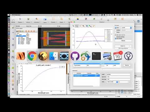
http://www.youtube.com/watch?v=qWtbPcVbAbY
Load measurement data from GitHub, save to disk, and plot
Identify opt_in circuit, using one of:
- selected opt_in Text objects
- GUI
- All - first option
- Individual - selected
Query GitHub to find measurement data for opt_in label(s)
Get data, one of:
- All
- Individual
Identify opt_in labels, and find the circuit(s) , using one of:
- selected opt_in Text objects
- GUI
- All - first option
- Individual - selected
Fetch measurement data from GitHub Run simulation
Plot data together